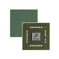
MPC8544VTALF Freescale Semiconductor, MPC8544VTALF Datasheet - Page 271

MPC8544VTALF
Manufacturer Part Number
MPC8544VTALF
Description
MPU POWERQUICC III 783-PBGA
Manufacturer
Freescale Semiconductor
Datasheets
1.MPC8544VTALF.pdf
(117 pages)
2.MPC8544VTALF.pdf
(2 pages)
3.MPC8544VTALF.pdf
(1340 pages)
Specifications of MPC8544VTALF
Processor Type
MPC85xx PowerQUICC III 32-Bit
Speed
667MHz
Voltage
1V
Mounting Type
Surface Mount
Package / Case
783-FCPBGA
Processor Series
MPC85xx
Core
e500
Data Bus Width
32 bit
Maximum Clock Frequency
667 MHz
Maximum Operating Temperature
+ 105 C
Mounting Style
SMD/SMT
Data Ram Size
32 KB
I/o Voltage
1.8 V, 3.3 V
Interface Type
I2C, HSSI, DUART
Minimum Operating Temperature
0 C
Lead Free Status / RoHS Status
Lead free / RoHS Compliant
Features
-
Lead Free Status / Rohs Status
Lead free / RoHS Compliant
Available stocks
Company
Part Number
Manufacturer
Quantity
Price
Company:
Part Number:
MPC8544VTALF
Manufacturer:
Freescale Semiconductor
Quantity:
10 000
Company:
Part Number:
MPC8544VTALFA
Manufacturer:
Freescale Semiconductor
Quantity:
10 000
- Current page: 271 of 1340
- Download datasheet (12Mb)
Chapter 7
L2 Look-Aside Cache/SRAM
This chapter describes the organization of the on-chip L2/SRAM, cache coherency rules, cache line
replacement algorithm, cache control instructions, and various cache operations. It also describes the
interaction between the L2/SRAM and the e500 core complex.
7.1
The integrated 256-Kbyte L2 cache is organized as 1024 eight-way sets of 32-byte cache lines based on
36-bit physical addresses, as shown in
The SRAM can be configured with memory-mapped registers as externally accessible memory-mapped
SRAM in addition to or instead of cache. The L2 cache can operate in the following modes, described in
Section 7.2, “L2 Cache and SRAM
Freescale Semiconductor
•
•
•
Full cache mode (256-Kbyte cache).
Full memory-mapped SRAM mode (256-Kbyte SRAM mapped as a single 256-Kbyte block or
two 128-Kbyte blocks)
Partial SRAM and partial cache mode, in which one eighth, one quarter, or one half the total
on-chip memory can be allocated to 1 or 2 SRAM regions.
L2 Cache Overview
MPC8544E PowerQUICC III Integrated Host Processor Family Reference Manual, Rev. 1
Independently programmable
WR IN
as L2 cache or SRAM
Four 64-Kbyte banks
L2 Cache/SRAM
256-Kbyte
(8-way)
DOUT
Figure 7-1. L2 Cache/SRAM Configuration
Organization”:
RD IN
Figure
128
7-1.
128
64
32-Kbyte L1
Data Cache
e500 Core Complex
Core Complex Bus
Coherency Module
RD1
e500 Core
RD2
Instruction Cache
32-Kbyte L1
WR
7-1
Related parts for MPC8544VTALF
Image
Part Number
Description
Manufacturer
Datasheet
Request
R
Part Number:
Description:
Manufacturer:
Freescale Semiconductor, Inc
Datasheet:
Part Number:
Description:
Manufacturer:
Freescale Semiconductor, Inc
Datasheet:
Part Number:
Description:
Manufacturer:
Freescale Semiconductor, Inc
Datasheet:
Part Number:
Description:
Manufacturer:
Freescale Semiconductor, Inc
Datasheet:
Part Number:
Description:
Manufacturer:
Freescale Semiconductor, Inc
Datasheet:
Part Number:
Description:
Manufacturer:
Freescale Semiconductor, Inc
Datasheet:
Part Number:
Description:
Manufacturer:
Freescale Semiconductor, Inc
Datasheet:
Part Number:
Description:
Manufacturer:
Freescale Semiconductor, Inc
Datasheet:
Part Number:
Description:
Manufacturer:
Freescale Semiconductor, Inc
Datasheet:
Part Number:
Description:
Manufacturer:
Freescale Semiconductor, Inc
Datasheet:
Part Number:
Description:
Manufacturer:
Freescale Semiconductor, Inc
Datasheet:
Part Number:
Description:
Manufacturer:
Freescale Semiconductor, Inc
Datasheet:
Part Number:
Description:
Manufacturer:
Freescale Semiconductor, Inc
Datasheet:
Part Number:
Description:
Manufacturer:
Freescale Semiconductor, Inc
Datasheet:
Part Number:
Description:
Manufacturer:
Freescale Semiconductor, Inc
Datasheet:


