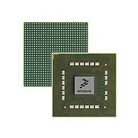
MPC8544VTALF Freescale Semiconductor, MPC8544VTALF Datasheet - Page 940

MPC8544VTALF
Manufacturer Part Number
MPC8544VTALF
Description
MPU POWERQUICC III 783-PBGA
Manufacturer
Freescale Semiconductor
Datasheets
1.MPC8544VTALF.pdf
(117 pages)
2.MPC8544VTALF.pdf
(2 pages)
3.MPC8544VTALF.pdf
(1340 pages)
Specifications of MPC8544VTALF
Processor Type
MPC85xx PowerQUICC III 32-Bit
Speed
667MHz
Voltage
1V
Mounting Type
Surface Mount
Package / Case
783-FCPBGA
Processor Series
MPC85xx
Core
e500
Data Bus Width
32 bit
Maximum Clock Frequency
667 MHz
Maximum Operating Temperature
+ 105 C
Mounting Style
SMD/SMT
Data Ram Size
32 KB
I/o Voltage
1.8 V, 3.3 V
Interface Type
I2C, HSSI, DUART
Minimum Operating Temperature
0 C
Lead Free Status / RoHS Status
Lead free / RoHS Compliant
Features
-
Lead Free Status / Rohs Status
Lead free / RoHS Compliant
Available stocks
Company
Part Number
Manufacturer
Quantity
Price
Company:
Part Number:
MPC8544VTALF
Manufacturer:
Freescale Semiconductor
Quantity:
10 000
Company:
Part Number:
MPC8544VTALFA
Manufacturer:
Freescale Semiconductor
Quantity:
10 000
- Current page: 940 of 1340
- Download datasheet (12Mb)
Enhanced Three-Speed Ethernet Controllers
15-208
Other information about the link is also returned. (Extend Status, No pre, Remote Fault, An Ability, Link status, extend
Set up the MII Mgmt for a read cycle to PHY MII Mgmt register (write the PHY address and Register address),
read the MII Mgmt AN Link Partner Base Page Ability register and check bits 9 and 10. (Half and Full Duplex)
MII Mgmt AN Link Partner Base Page Ability ---> [0000_0000_0000_0000_0000_000x_1110_0000]
read the MII Mgmt AN Expansion register and check bits 13 and 14 (NP Able and Page Rx’d)
MPC8544E PowerQUICC III Integrated Host Processor Family Reference Manual, Rev. 1
The PHY Status control register is at address 0x1 and in this case the PHY Address is 0x10.
Perform an MII Mgmt read cycle of AN Link Partner Base Page Ability Register. (Optional)
(Uses the PHY address (0x10) and Register address (6) placed in MIIMADD register),
(Uses the PHY address (0x10) and Register address (5) placed in MIIMADD register),
(Uses the PHY address (2) and Register address (2) placed in MIIMADD register),
MII Mgmt AN Expansion ---> [0000_0000_0000_0000_0000_0000_0000_0110]
MII Mgmt AN Expansion ---> [0000_0000_0000_0000_0000_0000_0000_0110]
Table 15-169. SGMII Mode Register Initialization Steps (continued)
TBASE0–TBASE7[LLLL_LLLL_LLLL_LLLL_LLLL_LLLL_LLLL_L000]
Setup MIIMADD[0000_0000_0000_0000_0001_0000_0000_0110]
Setup MIIMADD[0000_0000_0000_0000_0001_0000_0000_0101]
MACnADDR1/2[0000_0000_0000_0000_0000_0000_0000_0000]
Initialize (Empty) Transmit Descriptor ring and fill buffers with Data
MIIMIND ---> [0000_0000_0000_0000_0000_0000_0000_0000]
DMACTRL[0000_0000_0000_0000_0000_0000_0000_0000]
MIIMADD[0000_0000_0000_0000_0001_0000_0000_0001]
GADDR n [0000_0000_0000_0000_0000_0000_0000_0000]
Perform an MII Mgmt read cycle of AN Expansion Register.
IEVENT[0000_0000_0000_0000_0000_0000_0000_0000]
RCTRL[0000_0000_0000_0000_0000_0000_0000_0000]
IMASK[0000_0000_0000_0000_0000_0000_0000_0000]
Read MII Mgmt Indicator register and check for Busy = 0,
read the MIIMSTAT register and check bit 10 (AN Done)
Check to see if PHY has completed Auto-Negotiation.
Perform an MII Mgmt read cycle of Status Register.
This indicates that the write cycle was completed.
Check to see if MII Mgmt write is complete.
Initialize MACnADDR1/2 (Optional)
Initialize DMACTRL (Optional)
Clear MIIMCOM[Read Cycle]
Clear MIIMCOM[Read Cycle]
Clear MIIMCOM[Read Cycle]
Initialize GADDR n (Optional)
Initialize TBASE0–TBASE7,
Set MIIMCOM[Read Cycle]
When MIIMIND[BUSY] = 0,
Set MIIMCOM[Read Cycle]
When MIIMIND[BUSY] = 0,
Set MIIMCOM[Read Cycle]
When MIIMIND[BUSY] = 0,
Initialize RCTRL (Optional)
Initialize IMASK (Optional)
Clear IEVENT register,
Ability)
Freescale Semiconductor
Related parts for MPC8544VTALF
Image
Part Number
Description
Manufacturer
Datasheet
Request
R
Part Number:
Description:
Manufacturer:
Freescale Semiconductor, Inc
Datasheet:
Part Number:
Description:
Manufacturer:
Freescale Semiconductor, Inc
Datasheet:
Part Number:
Description:
Manufacturer:
Freescale Semiconductor, Inc
Datasheet:
Part Number:
Description:
Manufacturer:
Freescale Semiconductor, Inc
Datasheet:
Part Number:
Description:
Manufacturer:
Freescale Semiconductor, Inc
Datasheet:
Part Number:
Description:
Manufacturer:
Freescale Semiconductor, Inc
Datasheet:
Part Number:
Description:
Manufacturer:
Freescale Semiconductor, Inc
Datasheet:
Part Number:
Description:
Manufacturer:
Freescale Semiconductor, Inc
Datasheet:
Part Number:
Description:
Manufacturer:
Freescale Semiconductor, Inc
Datasheet:
Part Number:
Description:
Manufacturer:
Freescale Semiconductor, Inc
Datasheet:
Part Number:
Description:
Manufacturer:
Freescale Semiconductor, Inc
Datasheet:
Part Number:
Description:
Manufacturer:
Freescale Semiconductor, Inc
Datasheet:
Part Number:
Description:
Manufacturer:
Freescale Semiconductor, Inc
Datasheet:
Part Number:
Description:
Manufacturer:
Freescale Semiconductor, Inc
Datasheet:
Part Number:
Description:
Manufacturer:
Freescale Semiconductor, Inc
Datasheet:


