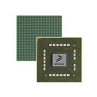
MPC8544VTALF Freescale Semiconductor, MPC8544VTALF Datasheet - Page 608

MPC8544VTALF
Manufacturer Part Number
MPC8544VTALF
Description
MPU POWERQUICC III 783-PBGA
Manufacturer
Freescale Semiconductor
Datasheets
1.MPC8544VTALF.pdf
(117 pages)
2.MPC8544VTALF.pdf
(2 pages)
3.MPC8544VTALF.pdf
(1340 pages)
Specifications of MPC8544VTALF
Processor Type
MPC85xx PowerQUICC III 32-Bit
Speed
667MHz
Voltage
1V
Mounting Type
Surface Mount
Package / Case
783-FCPBGA
Processor Series
MPC85xx
Core
e500
Data Bus Width
32 bit
Maximum Clock Frequency
667 MHz
Maximum Operating Temperature
+ 105 C
Mounting Style
SMD/SMT
Data Ram Size
32 KB
I/o Voltage
1.8 V, 3.3 V
Interface Type
I2C, HSSI, DUART
Minimum Operating Temperature
0 C
Lead Free Status / RoHS Status
Lead free / RoHS Compliant
Features
-
Lead Free Status / Rohs Status
Lead free / RoHS Compliant
Available stocks
Company
Part Number
Manufacturer
Quantity
Price
Company:
Part Number:
MPC8544VTALF
Manufacturer:
Freescale Semiconductor
Quantity:
10 000
Company:
Part Number:
MPC8544VTALFA
Manufacturer:
Freescale Semiconductor
Quantity:
10 000
- Current page: 608 of 1340
- Download datasheet (12Mb)
DUART
Table 13-12
13.3.1.7
The ULCRs specify the data format for the UART bus and set the divisor latch access bit ULCR[DLAB],
which controls the ability to access the divisor latch least and most significant bit registers and the alternate
function register.
After initializing the ULCR, the software should not re-write the ULCR when valid transfers on the UART
bus are active. The software should not re-write the ULCR until the last STOP bit has been received and
there are no new characters being transferred on the bus.
The stick parity bit, ULCR[SP], assigns a set parity value for the parity bit time slot sent on the UART bus.
The set value is defined as mark parity (logic 1) or space parity (logic 0). ULCR[PEN] and ULCR[EPS]
help determine the set parity value. See
number of STOP bits to be sent at the end of the data transfer. The receiver only checks the first STOP bit,
regardless of the number of STOP bits selected. The word length select bits (1 and 0) define the number
of data bits that are transmitted or received as a serial character. The word length does not include START,
parity, and STOP bits.
13-12
Bits
0–1
2–3
4
5
6
7
Name
DMS
RFR
TFR
FEN
RTL
—
describes the fields of the UFCRs.
MPC8544E PowerQUICC III Integrated Host Processor Family Reference Manual, Rev. 1
Receiver trigger level. A received data available interrupt occurs when UIER[ERDAI] is set and the number
of bytes in the receiver FIFO equals the designated interrupt trigger level as follows:
00 1 byte
01 4 bytes
10 8 bytes
11 14 bytes
Reserved
DMA mode select. See
0 UDSR[RXRDY] and UDSR[TXRDY] bits are in mode 0.
1 UDSR[RXRDY] and UDSR[TXRDY] bits are in mode 1 if UFCR[FEN] = 1.
Transmitter FIFO reset
0 No action
1 Clears all bytes in the transmitter FIFO and resets the FIFO counter/pointer to 0
Receiver FIFO reset
0 No action
1 Clears all bytes in the receiver FIFO and resets the FIFO counter/pointer to 0
FIFO enable
0 FIFOs are disabled and cleared
1 Enables the transmitter and receiver FIFOs
Line Control Registers (ULCR0, ULCR1)
Table 13-12. UFCR Field Descriptions
Section 13.4.5.2, “DMA Mode Select,”
Table 13-14
for more information. ULCR[NSTB], defines the
Description
for more information.
Freescale Semiconductor
Related parts for MPC8544VTALF
Image
Part Number
Description
Manufacturer
Datasheet
Request
R
Part Number:
Description:
Manufacturer:
Freescale Semiconductor, Inc
Datasheet:
Part Number:
Description:
Manufacturer:
Freescale Semiconductor, Inc
Datasheet:
Part Number:
Description:
Manufacturer:
Freescale Semiconductor, Inc
Datasheet:
Part Number:
Description:
Manufacturer:
Freescale Semiconductor, Inc
Datasheet:
Part Number:
Description:
Manufacturer:
Freescale Semiconductor, Inc
Datasheet:
Part Number:
Description:
Manufacturer:
Freescale Semiconductor, Inc
Datasheet:
Part Number:
Description:
Manufacturer:
Freescale Semiconductor, Inc
Datasheet:
Part Number:
Description:
Manufacturer:
Freescale Semiconductor, Inc
Datasheet:
Part Number:
Description:
Manufacturer:
Freescale Semiconductor, Inc
Datasheet:
Part Number:
Description:
Manufacturer:
Freescale Semiconductor, Inc
Datasheet:
Part Number:
Description:
Manufacturer:
Freescale Semiconductor, Inc
Datasheet:
Part Number:
Description:
Manufacturer:
Freescale Semiconductor, Inc
Datasheet:
Part Number:
Description:
Manufacturer:
Freescale Semiconductor, Inc
Datasheet:
Part Number:
Description:
Manufacturer:
Freescale Semiconductor, Inc
Datasheet:
Part Number:
Description:
Manufacturer:
Freescale Semiconductor, Inc
Datasheet:


