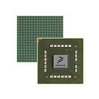
MPC8544VTALF Freescale Semiconductor, MPC8544VTALF Datasheet - Page 678

MPC8544VTALF
Manufacturer Part Number
MPC8544VTALF
Description
MPU POWERQUICC III 783-PBGA
Manufacturer
Freescale Semiconductor
Datasheets
1.MPC8544VTALF.pdf
(117 pages)
2.MPC8544VTALF.pdf
(2 pages)
3.MPC8544VTALF.pdf
(1340 pages)
Specifications of MPC8544VTALF
Processor Type
MPC85xx PowerQUICC III 32-Bit
Speed
667MHz
Voltage
1V
Mounting Type
Surface Mount
Package / Case
783-FCPBGA
Processor Series
MPC85xx
Core
e500
Data Bus Width
32 bit
Maximum Clock Frequency
667 MHz
Maximum Operating Temperature
+ 105 C
Mounting Style
SMD/SMT
Data Ram Size
32 KB
I/o Voltage
1.8 V, 3.3 V
Interface Type
I2C, HSSI, DUART
Minimum Operating Temperature
0 C
Lead Free Status / RoHS Status
Lead free / RoHS Compliant
Features
-
Lead Free Status / Rohs Status
Lead free / RoHS Compliant
Available stocks
Company
Part Number
Manufacturer
Quantity
Price
Company:
Part Number:
MPC8544VTALF
Manufacturer:
Freescale Semiconductor
Quantity:
10 000
Company:
Part Number:
MPC8544VTALFA
Manufacturer:
Freescale Semiconductor
Quantity:
10 000
- Current page: 678 of 1340
- Download datasheet (12Mb)
Local Bus Controller
between memory accesses and refresh cycles. The period of the refresh interval must be greater than the
access time to ensure that read and write operations complete successfully.
There are two levels of refresh request priority—low and high. The low priority request is generated as
soon as the refresh timer expires; this request is granted only if no other requests to the memory controller
are pending. If the request is not granted (memory controller is busy) and the refresh timer expires two
more times, the request becomes high priority and is served when the current memory controller operation
finishes.
14.4.3.11.1
The SDRAM memory controller implements bank staggering for the auto refresh function. This reduces
instantaneous current consumption for memory refresh operations.
After a refresh request is granted, the memory controller begins issuing an AUTO-REFRESH command
to each device associated with the refresh timer. After a refresh command is issued to an SDRAM device,
the memory controller waits for the number of bus clock cycles programmed in the S
DRAM machine’s mode register (LSDMR[RFCR]) before issuing any subsequent ACTIVATE command
to the same device. To avoid violating SDRAM device timing constraints, the user should ensure that the
refresh request interval, defined by LSRT and MRTPR, is greater than the refresh recovery interval,
defined by LSDMR[RFCR].
14.4.4
UPMs are flexible interfaces that connect to a wide range of memory devices. At the heart of each UPM
is an internal RAM array that specifies the logical value driven on the external memory control signals
(LCSn, LBS[0:3], and LGPL[0:5]) for a given clock cycle. Each word in the RAM array provides bits that
allow a memory access to be controlled with a resolution of up to one quarter of the external bus clock
period on the byte select and chip select lines.
14-58
LSDDQM[0:3]
LAD[0:31]
LSDRAS
LSDCAS
LSDWE
LCLK
LCS1
LCS2
LCS3
LCS4
LALE
User-Programmable Machines (UPMs)
MPC8544E PowerQUICC III Integrated Host Processor Family Reference Manual, Rev. 1
TA
SDRAM Refresh Timing
Figure 14-52. SDRAM Bank-Staggered Auto-Refresh Timing
Auto
Ref
Auto
Ref
Auto
Ref
Z
Auto
Ref
1111
LSDMR[RFCR]
ROW ADD
X
Activate
COL ADD
Freescale Semiconductor
0000
D0
1111
Z
Related parts for MPC8544VTALF
Image
Part Number
Description
Manufacturer
Datasheet
Request
R
Part Number:
Description:
Manufacturer:
Freescale Semiconductor, Inc
Datasheet:
Part Number:
Description:
Manufacturer:
Freescale Semiconductor, Inc
Datasheet:
Part Number:
Description:
Manufacturer:
Freescale Semiconductor, Inc
Datasheet:
Part Number:
Description:
Manufacturer:
Freescale Semiconductor, Inc
Datasheet:
Part Number:
Description:
Manufacturer:
Freescale Semiconductor, Inc
Datasheet:
Part Number:
Description:
Manufacturer:
Freescale Semiconductor, Inc
Datasheet:
Part Number:
Description:
Manufacturer:
Freescale Semiconductor, Inc
Datasheet:
Part Number:
Description:
Manufacturer:
Freescale Semiconductor, Inc
Datasheet:
Part Number:
Description:
Manufacturer:
Freescale Semiconductor, Inc
Datasheet:
Part Number:
Description:
Manufacturer:
Freescale Semiconductor, Inc
Datasheet:
Part Number:
Description:
Manufacturer:
Freescale Semiconductor, Inc
Datasheet:
Part Number:
Description:
Manufacturer:
Freescale Semiconductor, Inc
Datasheet:
Part Number:
Description:
Manufacturer:
Freescale Semiconductor, Inc
Datasheet:
Part Number:
Description:
Manufacturer:
Freescale Semiconductor, Inc
Datasheet:
Part Number:
Description:
Manufacturer:
Freescale Semiconductor, Inc
Datasheet:


