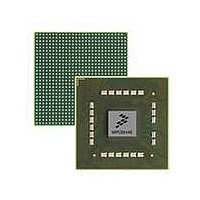
MPC8544VTALF Freescale Semiconductor, MPC8544VTALF Datasheet - Page 458

MPC8544VTALF
Manufacturer Part Number
MPC8544VTALF
Description
MPU POWERQUICC III 783-PBGA
Manufacturer
Freescale Semiconductor
Datasheets
1.MPC8544VTALF.pdf
(117 pages)
2.MPC8544VTALF.pdf
(2 pages)
3.MPC8544VTALF.pdf
(1340 pages)
Specifications of MPC8544VTALF
Processor Type
MPC85xx PowerQUICC III 32-Bit
Speed
667MHz
Voltage
1V
Mounting Type
Surface Mount
Package / Case
783-FCPBGA
Processor Series
MPC85xx
Core
e500
Data Bus Width
32 bit
Maximum Clock Frequency
667 MHz
Maximum Operating Temperature
+ 105 C
Mounting Style
SMD/SMT
Data Ram Size
32 KB
I/o Voltage
1.8 V, 3.3 V
Interface Type
I2C, HSSI, DUART
Minimum Operating Temperature
0 C
Lead Free Status / RoHS Status
Lead free / RoHS Compliant
Features
-
Lead Free Status / Rohs Status
Lead free / RoHS Compliant
Available stocks
Company
Part Number
Manufacturer
Quantity
Price
Company:
Part Number:
MPC8544VTALF
Manufacturer:
Freescale Semiconductor
Quantity:
10 000
Company:
Part Number:
MPC8544VTALFA
Manufacturer:
Freescale Semiconductor
Quantity:
10 000
- Current page: 458 of 1340
- Download datasheet (12Mb)
I
11.3
Table 11-3
to the complete description of each register. Note that the full register address is comprised of CCSRBAR
together with the block base address and offset listed in
are defined for both I
offset 0x100. The registers for I
the registers are the same for I
In this table and in the register figures and field descriptions, the following access definitions apply:
11-4
2
C Interfaces
IIC n _SCL
IIC n _SDA
Signal
•
•
•
•
•
Reserved fields are always ignored for the purposes of determining access type.
R/W, R, and W (read/write, read only, and write only) indicate that all the non-reserved fields in a
register have the same access type.
w1c indicates that all of the non-reserved fields in a register are cleared by writing ones to them.
Mixed indicates a combination of access types.
Special is used when no other category applies. In this case the register figure and field description
table should be read carefully.
Memory Map/Register Definition
lists the I
I/O
I/O Serial clock. Performs as an input when the device is programmed as an I
I/O Serial data. Performs as an input when the device is in a receiving mode. SDA also performs as an output
O
O
I
I
MPC8544E PowerQUICC III Integrated Host Processor Family Reference Manual, Rev. 1
output when the device is programmed as an I
As outputs for the bidirectional serial clock, these signals operate as described below.
As inputs for the bidirectional serial clock, these signals operate as described below.
signal when the device is transmitting (as an I
As outputs for the bidirectional serial data, these signals operate as described below.
As inputs for the bidirectional serial data, these signals operate as described below.
Meaning
Meaning
Meaning
Meaning
State
State
State
State
2
2
C-specific registers and their offsets. It lists the offset, name, and a cross-reference
C interfaces. That is, I
Table 11-2. I
Asserted/Negated—Driven along with SDA as the clock for the data.
Asserted/Negated—The I
Asserted/Negated— Data is driven.
Asserted/Negated—Used to receive data from other devices. The bus is assumed to be busy when
is assumed to be busy when this signal is detected low.
SDA is detected low.
2
C2 except that the offsets change from 0x0nn to 0x1nn.
2
C1 are listed in
2
C Interface Signal—Detailed Signal Descriptions
2
C1 starts at address offset 0x000, and I
2
C unit uses this signal to synchronize incoming data on SDA. The bus
Table
2
2
C master or a slave).
C master.
11-3, but the registers for I
Description
Table
11-3. The offsets to the memory map table
2
C slave. SCL also performs as an
2
C2 are not. Note that
Freescale Semiconductor
2
C2 starts at address
Related parts for MPC8544VTALF
Image
Part Number
Description
Manufacturer
Datasheet
Request
R
Part Number:
Description:
Manufacturer:
Freescale Semiconductor, Inc
Datasheet:
Part Number:
Description:
Manufacturer:
Freescale Semiconductor, Inc
Datasheet:
Part Number:
Description:
Manufacturer:
Freescale Semiconductor, Inc
Datasheet:
Part Number:
Description:
Manufacturer:
Freescale Semiconductor, Inc
Datasheet:
Part Number:
Description:
Manufacturer:
Freescale Semiconductor, Inc
Datasheet:
Part Number:
Description:
Manufacturer:
Freescale Semiconductor, Inc
Datasheet:
Part Number:
Description:
Manufacturer:
Freescale Semiconductor, Inc
Datasheet:
Part Number:
Description:
Manufacturer:
Freescale Semiconductor, Inc
Datasheet:
Part Number:
Description:
Manufacturer:
Freescale Semiconductor, Inc
Datasheet:
Part Number:
Description:
Manufacturer:
Freescale Semiconductor, Inc
Datasheet:
Part Number:
Description:
Manufacturer:
Freescale Semiconductor, Inc
Datasheet:
Part Number:
Description:
Manufacturer:
Freescale Semiconductor, Inc
Datasheet:
Part Number:
Description:
Manufacturer:
Freescale Semiconductor, Inc
Datasheet:
Part Number:
Description:
Manufacturer:
Freescale Semiconductor, Inc
Datasheet:
Part Number:
Description:
Manufacturer:
Freescale Semiconductor, Inc
Datasheet:


