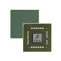
MPC8544VTALF Freescale Semiconductor, MPC8544VTALF Datasheet - Page 992

MPC8544VTALF
Manufacturer Part Number
MPC8544VTALF
Description
MPU POWERQUICC III 783-PBGA
Manufacturer
Freescale Semiconductor
Datasheets
1.MPC8544VTALF.pdf
(117 pages)
2.MPC8544VTALF.pdf
(2 pages)
3.MPC8544VTALF.pdf
(1340 pages)
Specifications of MPC8544VTALF
Processor Type
MPC85xx PowerQUICC III 32-Bit
Speed
667MHz
Voltage
1V
Mounting Type
Surface Mount
Package / Case
783-FCPBGA
Processor Series
MPC85xx
Core
e500
Data Bus Width
32 bit
Maximum Clock Frequency
667 MHz
Maximum Operating Temperature
+ 105 C
Mounting Style
SMD/SMT
Data Ram Size
32 KB
I/o Voltage
1.8 V, 3.3 V
Interface Type
I2C, HSSI, DUART
Minimum Operating Temperature
0 C
Lead Free Status / RoHS Status
Lead free / RoHS Compliant
Features
-
Lead Free Status / Rohs Status
Lead free / RoHS Compliant
Available stocks
Company
Part Number
Manufacturer
Quantity
Price
Company:
Part Number:
MPC8544VTALF
Manufacturer:
Freescale Semiconductor
Quantity:
10 000
Company:
Part Number:
MPC8544VTALFA
Manufacturer:
Freescale Semiconductor
Quantity:
10 000
- Current page: 992 of 1340
- Download datasheet (12Mb)
PCI Bus Interface
17-8
PCI_GNT[4:0]
PCI_IDSEL
PCI_IRDY
Signal
MPC8544E PowerQUICC III Integrated Host Processor Family Reference Manual, Rev. 1
Table 17-2. PCI Interface Signals—Detailed Signal Descriptions (continued)
I/O
I/O Initiator ready. The initiator ready signal is both an input and output signal on this PCI controller.
O PCI bus grant. Output signals on this PCI controller when the arbiter is enabled. When the arbiter is
O As outputs for the bidirectional initiator ready, these signals operate as described below.
I Initialization device select. The initialization device select signal is an input signal on this PCI controller.
I As inputs for the bidirectional initiator ready, these signals operate as described below.
disabled PCI_GNT0 is an input signal. Note that PCI_GNT[ n ] is a point-to-point signal. Every master
has its own bus grant signal.
Also, note that these signals are also used as reset configuration signals as described in
“Power-On Reset Configuration."
It is used as a chip select during configuration read and write transactions.
Meaning
Meaning
Meaning
Meaning
Timing Assertion/Negation—As specified by PCI Local Bus Specification Rev 2.2
Timing Assertion/Negation—As specified by PCI Local Bus Specification Rev 2.2
Timing Assertion/Negation—As specified by PCI Local Bus Specification Rev 2.2
Timing Assertion/Negation—As specified by PCI Local Bus Specification Rev 2.2
State
State
State
State
Asserted—Indicates that this PCI controller has granted control of the PCI bus to agent n .
Negated—Indicates that this PCI controller has not granted control of the PCI bus to agent n .
Asserted—Indicates this PCI controller is being selected as a target of a configuration read
Negated—Indicates this PCI controller is not being selected as a target of configuration
Asserted—Indicates that this PCI controller, acting as a PCI master, can complete the
Negated—Indicates that the PCI target needs to wait before this PCI controller, acting as a
Asserted—Indicates another PCI master is able to complete the current data phase of a
Negated—If PCI_FRAME is asserted, indicates a wait cycle from another master. If
or write transactions.
read or write transactions.
current data phase of a PCI transaction. During a write, this PCI controller asserts
PCI_IRDY to indicate that valid data is present on the data bus. During a read, this
PCI controller asserts PCI_IRDY to indicate that it is prepared to accept data.
PCI master, can complete the current data phase. During a write, this PCI controller
negates PCI_IRDY to insert a wait cycle when it cannot provide valid data to the
target. During a read, this PCI controller negates PCI_IRDY to insert a wait cycle
when it cannot accept data from the target.
transaction.
PCI_FRAME is negated, indicates the PCI bus is idle.
Description
Freescale Semiconductor
Section 4.4.3,
Related parts for MPC8544VTALF
Image
Part Number
Description
Manufacturer
Datasheet
Request
R
Part Number:
Description:
Manufacturer:
Freescale Semiconductor, Inc
Datasheet:
Part Number:
Description:
Manufacturer:
Freescale Semiconductor, Inc
Datasheet:
Part Number:
Description:
Manufacturer:
Freescale Semiconductor, Inc
Datasheet:
Part Number:
Description:
Manufacturer:
Freescale Semiconductor, Inc
Datasheet:
Part Number:
Description:
Manufacturer:
Freescale Semiconductor, Inc
Datasheet:
Part Number:
Description:
Manufacturer:
Freescale Semiconductor, Inc
Datasheet:
Part Number:
Description:
Manufacturer:
Freescale Semiconductor, Inc
Datasheet:
Part Number:
Description:
Manufacturer:
Freescale Semiconductor, Inc
Datasheet:
Part Number:
Description:
Manufacturer:
Freescale Semiconductor, Inc
Datasheet:
Part Number:
Description:
Manufacturer:
Freescale Semiconductor, Inc
Datasheet:
Part Number:
Description:
Manufacturer:
Freescale Semiconductor, Inc
Datasheet:
Part Number:
Description:
Manufacturer:
Freescale Semiconductor, Inc
Datasheet:
Part Number:
Description:
Manufacturer:
Freescale Semiconductor, Inc
Datasheet:
Part Number:
Description:
Manufacturer:
Freescale Semiconductor, Inc
Datasheet:
Part Number:
Description:
Manufacturer:
Freescale Semiconductor, Inc
Datasheet:


