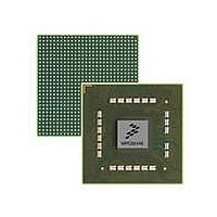
MPC8544VTALF Freescale Semiconductor, MPC8544VTALF Datasheet - Page 561

MPC8544VTALF
Manufacturer Part Number
MPC8544VTALF
Description
MPU POWERQUICC III 783-PBGA
Manufacturer
Freescale Semiconductor
Datasheets
1.MPC8544VTALF.pdf
(117 pages)
2.MPC8544VTALF.pdf
(2 pages)
3.MPC8544VTALF.pdf
(1340 pages)
Specifications of MPC8544VTALF
Processor Type
MPC85xx PowerQUICC III 32-Bit
Speed
667MHz
Voltage
1V
Mounting Type
Surface Mount
Package / Case
783-FCPBGA
Processor Series
MPC85xx
Core
e500
Data Bus Width
32 bit
Maximum Clock Frequency
667 MHz
Maximum Operating Temperature
+ 105 C
Mounting Style
SMD/SMT
Data Ram Size
32 KB
I/o Voltage
1.8 V, 3.3 V
Interface Type
I2C, HSSI, DUART
Minimum Operating Temperature
0 C
Lead Free Status / RoHS Status
Lead free / RoHS Compliant
Features
-
Lead Free Status / Rohs Status
Lead free / RoHS Compliant
Available stocks
Company
Part Number
Manufacturer
Quantity
Price
Company:
Part Number:
MPC8544VTALF
Manufacturer:
Freescale Semiconductor
Quantity:
10 000
Company:
Part Number:
MPC8544VTALFA
Manufacturer:
Freescale Semiconductor
Quantity:
10 000
- Current page: 561 of 1340
- Download datasheet (12Mb)
12.4.7.2
The KEU key size register, shown in
to 16 bytes. This register is cleared when the KEU is reset or re-initialized. If a key size is specified that
does not match the selected algorithm(s), an illegal key size error is generated.
12.4.7.3
The KEU data size register stores the number of bits to process in the final message word. Because Kasumi
allows for bit level granularity for encryption/decryption, there are no illegal data sizes. The proper bit
length of the message must be written to notify the KEU of any padding performed by the host. This
register is cleared when the KEU is reset or re-initialized.
Writing to this register signals the KEU to start processing data from the input FIFO as soon as it is
available. If the value of data size is modified during processing, a context error is generated.
Freescale Semiconductor
62–63
Address KEU 0x3_E008
Bits
59
60
61
Reset
W
R
Name
ALG
0
INT
PE
—
KEU Key Size Register (KEUKSR)
KEU Data Size Register (KEUDSR)
Process end of message. Enables final processing of last message block (F9 only).
0 Prevent final block processing (message incomplete)
1 Enable final block processing (message complete)
Note: For f9 operations, if the 3G frame (or message) is being processed as a whole (not split across multiple
Initialization. Enables initialization for a new message.
0 Prevent initialization
1 Enable initialization
Note: For F8 or F9 operations, if the 3G frame (or message) is being processed through a single descriptor, the
Reserved
Algorithm selection. Specifies the functions to perform.
00 Perform F8 function only
01 Reserved
10 F9 function only
11 Reserved
MPC8544E PowerQUICC III Integrated Host Processor Family Reference Manual, Rev. 1
descriptors), the process end of message bit should be set. If the frame is processed across multiple
descriptors, this bit should only be set on the descriptor performing f9 processing on the final message
block.
Initialization bit should be set. If the frame is split across multiple descriptors, this bit should only be set in
the descriptor that processes the first block of the message.
Table 12-44. KEU Mode Register Field Descriptions (continued)
Figure 12-58. KEU Key Size Register
Figure
12-58, stores the number of bytes in the key. It should be set
—
All zeros
Description
51 52
Security Engine (SEC) 2.1
Access: Read/Write
Key Size (Bytes)
12-81
63
Related parts for MPC8544VTALF
Image
Part Number
Description
Manufacturer
Datasheet
Request
R
Part Number:
Description:
Manufacturer:
Freescale Semiconductor, Inc
Datasheet:
Part Number:
Description:
Manufacturer:
Freescale Semiconductor, Inc
Datasheet:
Part Number:
Description:
Manufacturer:
Freescale Semiconductor, Inc
Datasheet:
Part Number:
Description:
Manufacturer:
Freescale Semiconductor, Inc
Datasheet:
Part Number:
Description:
Manufacturer:
Freescale Semiconductor, Inc
Datasheet:
Part Number:
Description:
Manufacturer:
Freescale Semiconductor, Inc
Datasheet:
Part Number:
Description:
Manufacturer:
Freescale Semiconductor, Inc
Datasheet:
Part Number:
Description:
Manufacturer:
Freescale Semiconductor, Inc
Datasheet:
Part Number:
Description:
Manufacturer:
Freescale Semiconductor, Inc
Datasheet:
Part Number:
Description:
Manufacturer:
Freescale Semiconductor, Inc
Datasheet:
Part Number:
Description:
Manufacturer:
Freescale Semiconductor, Inc
Datasheet:
Part Number:
Description:
Manufacturer:
Freescale Semiconductor, Inc
Datasheet:
Part Number:
Description:
Manufacturer:
Freescale Semiconductor, Inc
Datasheet:
Part Number:
Description:
Manufacturer:
Freescale Semiconductor, Inc
Datasheet:
Part Number:
Description:
Manufacturer:
Freescale Semiconductor, Inc
Datasheet:


