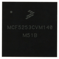
MCF5253CVM140 Freescale Semiconductor, MCF5253CVM140 Datasheet - Page 90

MCF5253CVM140
Manufacturer Part Number
MCF5253CVM140
Description
IC MPU 32BIT 140MHZ 225-MAPBGA
Manufacturer
Freescale Semiconductor
Series
MCF525xr
Datasheets
1.MCF5253VM140J.pdf
(34 pages)
2.MCF5253VM140J.pdf
(8 pages)
3.MCF5253VM140J.pdf
(648 pages)
4.MCF5253VM140J.pdf
(2 pages)
Specifications of MCF5253CVM140
Core Processor
Coldfire V2
Core Size
32-Bit
Speed
140MHz
Connectivity
CAN, EBI/EMI, I²C, QSPI, UART/USART, USB OTG
Peripherals
DMA, WDT
Program Memory Type
ROMless
Ram Size
128K x 8
Voltage - Supply (vcc/vdd)
1.08 V ~ 1.32 V
Data Converters
A/D 6x12b
Oscillator Type
External
Operating Temperature
-40°C ~ 85°C
Package / Case
225-MAPBGA
Family Name
MCF5xxx
Device Core
ColdFire V2
Device Core Size
32b
Frequency (max)
140MHz
Instruction Set Architecture
RISC
Supply Voltage 1 (typ)
1.2/3.3V
Operating Supply Voltage (max)
1.32/3.6V
Operating Supply Voltage (min)
1.08/3V
Operating Temp Range
-40C to 85C
Operating Temperature Classification
Industrial
Mounting
Surface Mount
Pin Count
225
Package Type
MA-BGA
Lead Free Status / RoHS Status
Lead free / RoHS Compliant
Number Of I /o
-
Eeprom Size
-
Program Memory Size
-
Lead Free Status / Rohs Status
Compliant
Available stocks
Company
Part Number
Manufacturer
Quantity
Price
Company:
Part Number:
MCF5253CVM140
Manufacturer:
FREESCALE
Quantity:
300
Company:
Part Number:
MCF5253CVM140
Manufacturer:
Freescale Semiconductor
Quantity:
10 000
Part Number:
MCF5253CVM140
Manufacturer:
FREESCALE
Quantity:
20 000
Company:
Part Number:
MCF5253CVM140J
Manufacturer:
Freescale Semiconductor
Quantity:
10 000
- MCF5253VM140J PDF datasheet
- MCF5253VM140J PDF datasheet #2
- MCF5253VM140J PDF datasheet #3
- MCF5253VM140J PDF datasheet #4
- Current page: 90 of 648
- Download datasheet (8Mb)
Instruction Cache
5.3
The instruction cache is a direct-mapped single-cycle memory, organized as 512 lines, each containing 16
Bytes. The memory storage consists of a 512-entry tag array (containing addresses and a valid bit), and the
data array containing 8 Kbyte of instruction data, organized as 2048 × 32 bits.
The two memory arrays are accessed in parallel: bits [12:4] of the instruction fetch address provide the
index into the tag array, and bits [12:2] addressing the data array. The tag array outputs the address mapped
to the given cache location along with the valid bit for the line. This address field is compared to bits
[31:12] of the instruction fetch address from the local bus to determine if a cache hit in the memory array
has occurred. If the desired address is mapped into the cache memory, the output of the data array is driven
onto the ColdFire core's local data bus completing the access in a single cycle.
The tag array maintains a single valid bit per line entry. Accordingly, only entire 16 byte lines are loaded
into the instruction cache.
The instruction cache also contains a 16 byte fill buffer that provides temporary storage for the last line
fetched in response to a cache miss. With each instruction fetch, the contents of the line fill buffer are
examined. Thus, each instruction fetch address examines both the tag memory array and the line fill buffer
to see if the desired address is mapped into either hardware resource. A cache hit in either the memory
array or the line-fill buffer is serviced in a single cycle. Because the line fill buffer maintains valid bits on
a longword basis, hits in the buffer can be serviced immediately without waiting for the entire line to be
fetched.
If the referenced address is not contained in the memory array or the line-fill buffer, the instruction cache
initiates the required external fetch operation. In most situations, this is a 16 byte line-sized burst reference.
The hardware implementation is a nonblocking design, meaning the ColdFire core's local bus is released
after the initial access of a miss. Thus, the cache or the SRAM module can service subsequent requests
while the remainder of the line is being fetched and loaded into the fill buffer.
5.4
The instruction cache is physically connected to the ColdFire core local bus, allowing it to service all
instruction fetches from the ColdFire core and certain memory fetches initiated by the debug module.
Typically, the debug module's memory references appear as supervisor data accesses but the unit can be
programmed to generate user-mode accesses and/or instruction fetches. The instruction cache processes
any instruction fetch access in the normal manner.
5.4.1
Because both the instruction cache and high-speed SRAM module are connected to the ColdFire core local
data bus, certain user-defined configurations can result in simultaneous instruction fetch processing.
If the referenced address is mapped into the SRAM module, that module will service the request in a single
cycle. In this case, data accessed from the instruction cache is simply discarded and no external memory
references are generated. If the address is not mapped into the SRAM space, the instruction cache handles
the request in the normal fashion.
5-2
Instruction Cache Physical Organization
Instruction Cache Operation
Interaction with Other Modules
MCF5253 Reference Manual, Rev. 1
Freescale Semiconductor
Related parts for MCF5253CVM140
Image
Part Number
Description
Manufacturer
Datasheet
Request
R
Part Number:
Description:
Mcf5253 Coldfire? Microprocessor Data Sheet
Manufacturer:
Freescale Semiconductor, Inc
Datasheet:
Part Number:
Description:
Manufacturer:
Freescale Semiconductor, Inc
Datasheet:
Part Number:
Description:
Manufacturer:
Freescale Semiconductor, Inc
Datasheet:
Part Number:
Description:
Manufacturer:
Freescale Semiconductor, Inc
Datasheet:
Part Number:
Description:
Manufacturer:
Freescale Semiconductor, Inc
Datasheet:
Part Number:
Description:
Manufacturer:
Freescale Semiconductor, Inc
Datasheet:
Part Number:
Description:
Manufacturer:
Freescale Semiconductor, Inc
Datasheet:
Part Number:
Description:
Manufacturer:
Freescale Semiconductor, Inc
Datasheet:
Part Number:
Description:
Manufacturer:
Freescale Semiconductor, Inc
Datasheet:
Part Number:
Description:
Manufacturer:
Freescale Semiconductor, Inc
Datasheet:
Part Number:
Description:
Manufacturer:
Freescale Semiconductor, Inc
Datasheet:
Part Number:
Description:
Manufacturer:
Freescale Semiconductor, Inc
Datasheet:
Part Number:
Description:
Manufacturer:
Freescale Semiconductor, Inc
Datasheet:
Part Number:
Description:
Manufacturer:
Freescale Semiconductor, Inc
Datasheet:
Part Number:
Description:
Manufacturer:
Freescale Semiconductor, Inc
Datasheet:


