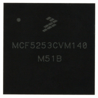
MCF5253CVM140 Freescale Semiconductor, MCF5253CVM140 Datasheet - Page 417

MCF5253CVM140
Manufacturer Part Number
MCF5253CVM140
Description
IC MPU 32BIT 140MHZ 225-MAPBGA
Manufacturer
Freescale Semiconductor
Series
MCF525xr
Datasheets
1.MCF5253VM140J.pdf
(34 pages)
2.MCF5253VM140J.pdf
(8 pages)
3.MCF5253VM140J.pdf
(648 pages)
4.MCF5253VM140J.pdf
(2 pages)
Specifications of MCF5253CVM140
Core Processor
Coldfire V2
Core Size
32-Bit
Speed
140MHz
Connectivity
CAN, EBI/EMI, I²C, QSPI, UART/USART, USB OTG
Peripherals
DMA, WDT
Program Memory Type
ROMless
Ram Size
128K x 8
Voltage - Supply (vcc/vdd)
1.08 V ~ 1.32 V
Data Converters
A/D 6x12b
Oscillator Type
External
Operating Temperature
-40°C ~ 85°C
Package / Case
225-MAPBGA
Family Name
MCF5xxx
Device Core
ColdFire V2
Device Core Size
32b
Frequency (max)
140MHz
Instruction Set Architecture
RISC
Supply Voltage 1 (typ)
1.2/3.3V
Operating Supply Voltage (max)
1.32/3.6V
Operating Supply Voltage (min)
1.08/3V
Operating Temp Range
-40C to 85C
Operating Temperature Classification
Industrial
Mounting
Surface Mount
Pin Count
225
Package Type
MA-BGA
Lead Free Status / RoHS Status
Lead free / RoHS Compliant
Number Of I /o
-
Eeprom Size
-
Program Memory Size
-
Lead Free Status / Rohs Status
Compliant
Available stocks
Company
Part Number
Manufacturer
Quantity
Price
Company:
Part Number:
MCF5253CVM140
Manufacturer:
FREESCALE
Quantity:
300
Company:
Part Number:
MCF5253CVM140
Manufacturer:
Freescale Semiconductor
Quantity:
10 000
Part Number:
MCF5253CVM140
Manufacturer:
FREESCALE
Quantity:
20 000
Company:
Part Number:
MCF5253CVM140J
Manufacturer:
Freescale Semiconductor
Quantity:
10 000
- MCF5253VM140J PDF datasheet
- MCF5253VM140J PDF datasheet #2
- MCF5253VM140J PDF datasheet #3
- MCF5253VM140J PDF datasheet #4
- Current page: 417 of 648
- Download datasheet (8Mb)
and other part identification data. The IDcode register has been implemented in accordance with IEEE
1149.1A so that the least significant bit of the shift register stage is set to logic 1 on the rising edge of TCK
following entry into the capture-DR state. Therefore, the first bit to be shifted out after selecting the IDcode
register is always a logic 1. The remaining 31-bits are also set to fixed values (see
Register”) on the rising edge of TCK following entry into the capture-DR state.
The IDCODE instruction is the default value placed in the instruction register when a JTAG reset is
accomplished by either asserting TRST or holding TMS high while clocking TCK through at least five
rising edges and the falling edge after the fifth rising edge. A JTAG reset will cause the TAP state machine
to enter the test-logic-reset state (normal operation of the TAP state machine into the test-logic-reset state
will also result in placing the default value of 1 into the instruction register). The shift register portion of
the instruction register is loaded with the default value of 1 when in the Capture-IR state and a rising edge
of TCK occurs.
21.5.1.3
The SAMPLE/PRELOAD instruction provides two separate functions. First, it obtains a sample of the
system data and control signals present at the MCF5253 input pins and just prior to the boundary scan cell
at the output pins. This sampling occurs on the rising edge of TCK in the capture-DR state when an
instruction encoding of 2 is resident in the instruction register. Users can observe this sampled data by
shifting it through the boundary-scan register to the output TDO by using the shift-DR state. Both the data
capture and the shift operation are transparent to system operation. Users are responsible for providing
some form of external synchronization to achieve meaningful results because there is no internal
synchronization between TCK and the SYSCLK.
The second function of the SAMPLE/PRELOAD instruction is to initialize the boundary scan register
update cells before selecting EXTEST or CLAMP. This is achieved by ignoring the data being shifted out
of the TDO pin while shifting in initialization data. The update-DR state in conjunction with the falling
edge of TCK can then transfer this data to the update cells. This data will be applied to the external output
pins when one of the instructions listed above is applied.
21.5.1.4
The CLAMP instruction selects the bypass register and asserts functional reset while simultaneously
forcing all output pins and bidirectional pins configured as outputs to the fixed values that are preloaded
and held in the boundary-scan update registers. This instruction enhances test efficiency by reducing the
overall shift path to a single bit (the bypass register) while conducting an EXTEST type of instruction
through the boundary-scan register. The CLAMP instruction becomes active on the falling edge of TCK
in the update-IR state when the data held in the instruction-shift register is equivalent to 3.
21.5.1.5
The HIGHZ instruction anticipates the need to backdrive the output pins and protect the input pins from
random toggling during circuit board testing. The HIGHZ instruction selects the bypass register, forcing
all output and bidirectional pins to the high-impedance state.
Freescale Semiconductor
SAMPLE/PRELOAD Instruction
CLAMP Instruction
HIGHZ Instruction
MCF5253 Reference Manual, Rev. 1
IEEE 1149.1 Test Access Port (JTAG)
Section 21.5.2, “ID Code
21-7
Related parts for MCF5253CVM140
Image
Part Number
Description
Manufacturer
Datasheet
Request
R
Part Number:
Description:
Mcf5253 Coldfire? Microprocessor Data Sheet
Manufacturer:
Freescale Semiconductor, Inc
Datasheet:
Part Number:
Description:
Manufacturer:
Freescale Semiconductor, Inc
Datasheet:
Part Number:
Description:
Manufacturer:
Freescale Semiconductor, Inc
Datasheet:
Part Number:
Description:
Manufacturer:
Freescale Semiconductor, Inc
Datasheet:
Part Number:
Description:
Manufacturer:
Freescale Semiconductor, Inc
Datasheet:
Part Number:
Description:
Manufacturer:
Freescale Semiconductor, Inc
Datasheet:
Part Number:
Description:
Manufacturer:
Freescale Semiconductor, Inc
Datasheet:
Part Number:
Description:
Manufacturer:
Freescale Semiconductor, Inc
Datasheet:
Part Number:
Description:
Manufacturer:
Freescale Semiconductor, Inc
Datasheet:
Part Number:
Description:
Manufacturer:
Freescale Semiconductor, Inc
Datasheet:
Part Number:
Description:
Manufacturer:
Freescale Semiconductor, Inc
Datasheet:
Part Number:
Description:
Manufacturer:
Freescale Semiconductor, Inc
Datasheet:
Part Number:
Description:
Manufacturer:
Freescale Semiconductor, Inc
Datasheet:
Part Number:
Description:
Manufacturer:
Freescale Semiconductor, Inc
Datasheet:
Part Number:
Description:
Manufacturer:
Freescale Semiconductor, Inc
Datasheet:


