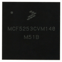
MCF5253CVM140 Freescale Semiconductor, MCF5253CVM140 Datasheet - Page 30

MCF5253CVM140
Manufacturer Part Number
MCF5253CVM140
Description
IC MPU 32BIT 140MHZ 225-MAPBGA
Manufacturer
Freescale Semiconductor
Series
MCF525xr
Datasheets
1.MCF5253VM140J.pdf
(34 pages)
2.MCF5253VM140J.pdf
(8 pages)
3.MCF5253VM140J.pdf
(648 pages)
4.MCF5253VM140J.pdf
(2 pages)
Specifications of MCF5253CVM140
Core Processor
Coldfire V2
Core Size
32-Bit
Speed
140MHz
Connectivity
CAN, EBI/EMI, I²C, QSPI, UART/USART, USB OTG
Peripherals
DMA, WDT
Program Memory Type
ROMless
Ram Size
128K x 8
Voltage - Supply (vcc/vdd)
1.08 V ~ 1.32 V
Data Converters
A/D 6x12b
Oscillator Type
External
Operating Temperature
-40°C ~ 85°C
Package / Case
225-MAPBGA
Family Name
MCF5xxx
Device Core
ColdFire V2
Device Core Size
32b
Frequency (max)
140MHz
Instruction Set Architecture
RISC
Supply Voltage 1 (typ)
1.2/3.3V
Operating Supply Voltage (max)
1.32/3.6V
Operating Supply Voltage (min)
1.08/3V
Operating Temp Range
-40C to 85C
Operating Temperature Classification
Industrial
Mounting
Surface Mount
Pin Count
225
Package Type
MA-BGA
Lead Free Status / RoHS Status
Lead free / RoHS Compliant
Number Of I /o
-
Eeprom Size
-
Program Memory Size
-
Lead Free Status / Rohs Status
Compliant
Available stocks
Company
Part Number
Manufacturer
Quantity
Price
Company:
Part Number:
MCF5253CVM140
Manufacturer:
FREESCALE
Quantity:
300
Company:
Part Number:
MCF5253CVM140
Manufacturer:
Freescale Semiconductor
Quantity:
10 000
Part Number:
MCF5253CVM140
Manufacturer:
FREESCALE
Quantity:
20 000
Company:
Part Number:
MCF5253CVM140J
Manufacturer:
Freescale Semiconductor
Quantity:
10 000
- MCF5253VM140J PDF datasheet
- MCF5253VM140J PDF datasheet #2
- MCF5253VM140J PDF datasheet #3
- MCF5253VM140J PDF datasheet #4
- Current page: 30 of 648
- Download datasheet (8Mb)
Conventions
This document uses the following notational conventions:
Definitions, Acronyms, and Abbreviations
The following list defines the acronyms and abbreviations used in this document.
DSP
JTAG
OnCE™
MIPS
SRAM
SDRAM block
SDRAM
SDRAM bank
References
The following sources were referenced to produce this book:
Register Summary
Figure 1
xxx
•
•
•
1. Low-Level Software Design Document for the PowerPC Architectural Simulator (delivery date to
2. Requirements Chapter of the Software Project Management Plan for the PowerPC
3. PowerPC User Instruction Set Architecture, Book I, Version 1.00, 5/19/92 (subtitled “Work in
4. PowerPC Virtual Environment Architecture, Book II, Version 1.00, 5/19/92 (subtitled “Work in
Courier monospaced type
data types, and directives.
Italic type indicates replaceable command parameters.
All source code examples are in C.
be determined)
Microarchitectural Timing Simulator (delivery date to be determined)
Progress”)
Progress”)
shows the key to the register fields and
digital signal processor
joint test access group
On-Chip Emulation
million instructions per second
static RAM
DRAM memory selected by SD_CS0/GPIO60 signals. The base address of the
block is programmed in the DRAM address and control register (DACR0).
RAMs that operate like asynchronous DRAMs but with a synchronous clock, a
pipelined, multiple-bank architecture, and faster speed.
An internal partition in an SDRAM device. For example, a 64-MBIT SDRAM
component might be configured as four 512K x 32 banks. Banks are selected
through the SDRAM component’s bank select lines.
indicate commands, command parameters, code examples, expressions,
MCF5253 Reference Manual, Rev. 1
Table 2
shows the register figure conventions.
Freescale Semiconductor
Related parts for MCF5253CVM140
Image
Part Number
Description
Manufacturer
Datasheet
Request
R
Part Number:
Description:
Mcf5253 Coldfire? Microprocessor Data Sheet
Manufacturer:
Freescale Semiconductor, Inc
Datasheet:
Part Number:
Description:
Manufacturer:
Freescale Semiconductor, Inc
Datasheet:
Part Number:
Description:
Manufacturer:
Freescale Semiconductor, Inc
Datasheet:
Part Number:
Description:
Manufacturer:
Freescale Semiconductor, Inc
Datasheet:
Part Number:
Description:
Manufacturer:
Freescale Semiconductor, Inc
Datasheet:
Part Number:
Description:
Manufacturer:
Freescale Semiconductor, Inc
Datasheet:
Part Number:
Description:
Manufacturer:
Freescale Semiconductor, Inc
Datasheet:
Part Number:
Description:
Manufacturer:
Freescale Semiconductor, Inc
Datasheet:
Part Number:
Description:
Manufacturer:
Freescale Semiconductor, Inc
Datasheet:
Part Number:
Description:
Manufacturer:
Freescale Semiconductor, Inc
Datasheet:
Part Number:
Description:
Manufacturer:
Freescale Semiconductor, Inc
Datasheet:
Part Number:
Description:
Manufacturer:
Freescale Semiconductor, Inc
Datasheet:
Part Number:
Description:
Manufacturer:
Freescale Semiconductor, Inc
Datasheet:
Part Number:
Description:
Manufacturer:
Freescale Semiconductor, Inc
Datasheet:
Part Number:
Description:
Manufacturer:
Freescale Semiconductor, Inc
Datasheet:


