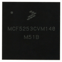
MCF5253CVM140 Freescale Semiconductor, MCF5253CVM140 Datasheet - Page 165

MCF5253CVM140
Manufacturer Part Number
MCF5253CVM140
Description
IC MPU 32BIT 140MHZ 225-MAPBGA
Manufacturer
Freescale Semiconductor
Series
MCF525xr
Datasheets
1.MCF5253VM140J.pdf
(34 pages)
2.MCF5253VM140J.pdf
(8 pages)
3.MCF5253VM140J.pdf
(648 pages)
4.MCF5253VM140J.pdf
(2 pages)
Specifications of MCF5253CVM140
Core Processor
Coldfire V2
Core Size
32-Bit
Speed
140MHz
Connectivity
CAN, EBI/EMI, I²C, QSPI, UART/USART, USB OTG
Peripherals
DMA, WDT
Program Memory Type
ROMless
Ram Size
128K x 8
Voltage - Supply (vcc/vdd)
1.08 V ~ 1.32 V
Data Converters
A/D 6x12b
Oscillator Type
External
Operating Temperature
-40°C ~ 85°C
Package / Case
225-MAPBGA
Family Name
MCF5xxx
Device Core
ColdFire V2
Device Core Size
32b
Frequency (max)
140MHz
Instruction Set Architecture
RISC
Supply Voltage 1 (typ)
1.2/3.3V
Operating Supply Voltage (max)
1.32/3.6V
Operating Supply Voltage (min)
1.08/3V
Operating Temp Range
-40C to 85C
Operating Temperature Classification
Industrial
Mounting
Surface Mount
Pin Count
225
Package Type
MA-BGA
Lead Free Status / RoHS Status
Lead free / RoHS Compliant
Number Of I /o
-
Eeprom Size
-
Program Memory Size
-
Lead Free Status / Rohs Status
Compliant
Available stocks
Company
Part Number
Manufacturer
Quantity
Price
Company:
Part Number:
MCF5253CVM140
Manufacturer:
FREESCALE
Quantity:
300
Company:
Part Number:
MCF5253CVM140
Manufacturer:
Freescale Semiconductor
Quantity:
10 000
Part Number:
MCF5253CVM140
Manufacturer:
FREESCALE
Quantity:
20 000
Company:
Part Number:
MCF5253CVM140J
Manufacturer:
Freescale Semiconductor
Quantity:
10 000
- MCF5253VM140J PDF datasheet
- MCF5253VM140J PDF datasheet #2
- MCF5253VM140J PDF datasheet #3
- MCF5253VM140J PDF datasheet #4
- Current page: 165 of 648
- Download datasheet (8Mb)
9.5.2.3
The SWSR is where the SWT servicing sequence should be written. To prevent an SWT timeout, users
should write a $55 followed by a $AA to this register. Both writes must be performed in the order listed
prior to the SWT timeout, but any number of instructions or accesses to the SWSR can be executed
between the two writes. If the SWT has already timed out, writing to this register will have no effect in
negating the SWT interrupt. The following register illustrates the SWSR programming model.
The SWSR is an 8-bit write-only register. At system reset, the contents of SWSR are uninitialized.
9.6
Executing the CPU HALT instruction stops the core but does not disable any system clocks.
9.7
This section contains the Default Bus Master Park register, the internal arbitration operation, and the
configuration of the PARK register bit.
9.7.1
The MPARK register determines the default bus master arbitration applied between internal transfers. This
arbitration is needed because there are two bus masters inside the MCF5253. One is the CPU, the other is
the DMA unit. Both can access internal registers within the MCF5253 peripherals.
MPARK register bit encoding.
The MPARK is an 8-bit read-write register.
Freescale Semiconductor
.
Address MBAR + $03
Address MBAR + $02
Reset
Reset
W
R
W
R
CPU HALT Instruction
MCF5253 Bus Arbitration Control Registers
Default Bus Master Park Register
SWSR7
Software Watchdog Service Register
SWIV7
7
–
0
7
Figure 9-12. Software Watchdog Interrupt Vector Register (SWIVR)
Figure 9-13. Software Watchdog Service Register (SWSR)
SWSR6
SWIV6
–
6
0
6
MCF5253 Reference Manual, Rev. 1
SWSR5
SWIV5
–
5
0
5
SWSR4
SWIV4
–
0
4
4
SWSR3
SWIV3
3
1
–
3
SWSR2
SWIV2
1
2
–
2
System Integration Module (SIM)
Table 9-14
SWIV1
SWSR1
Access: User read/write
Access: User read/write
1
1
–
1
shows the
SWIV0
SWSR0
1
0
0
–
9-21
Related parts for MCF5253CVM140
Image
Part Number
Description
Manufacturer
Datasheet
Request
R
Part Number:
Description:
Mcf5253 Coldfire? Microprocessor Data Sheet
Manufacturer:
Freescale Semiconductor, Inc
Datasheet:
Part Number:
Description:
Manufacturer:
Freescale Semiconductor, Inc
Datasheet:
Part Number:
Description:
Manufacturer:
Freescale Semiconductor, Inc
Datasheet:
Part Number:
Description:
Manufacturer:
Freescale Semiconductor, Inc
Datasheet:
Part Number:
Description:
Manufacturer:
Freescale Semiconductor, Inc
Datasheet:
Part Number:
Description:
Manufacturer:
Freescale Semiconductor, Inc
Datasheet:
Part Number:
Description:
Manufacturer:
Freescale Semiconductor, Inc
Datasheet:
Part Number:
Description:
Manufacturer:
Freescale Semiconductor, Inc
Datasheet:
Part Number:
Description:
Manufacturer:
Freescale Semiconductor, Inc
Datasheet:
Part Number:
Description:
Manufacturer:
Freescale Semiconductor, Inc
Datasheet:
Part Number:
Description:
Manufacturer:
Freescale Semiconductor, Inc
Datasheet:
Part Number:
Description:
Manufacturer:
Freescale Semiconductor, Inc
Datasheet:
Part Number:
Description:
Manufacturer:
Freescale Semiconductor, Inc
Datasheet:
Part Number:
Description:
Manufacturer:
Freescale Semiconductor, Inc
Datasheet:
Part Number:
Description:
Manufacturer:
Freescale Semiconductor, Inc
Datasheet:


