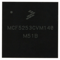
MCF5253CVM140 Freescale Semiconductor, MCF5253CVM140 Datasheet - Page 84

MCF5253CVM140
Manufacturer Part Number
MCF5253CVM140
Description
IC MPU 32BIT 140MHZ 225-MAPBGA
Manufacturer
Freescale Semiconductor
Series
MCF525xr
Datasheets
1.MCF5253VM140J.pdf
(34 pages)
2.MCF5253VM140J.pdf
(8 pages)
3.MCF5253VM140J.pdf
(648 pages)
4.MCF5253VM140J.pdf
(2 pages)
Specifications of MCF5253CVM140
Core Processor
Coldfire V2
Core Size
32-Bit
Speed
140MHz
Connectivity
CAN, EBI/EMI, I²C, QSPI, UART/USART, USB OTG
Peripherals
DMA, WDT
Program Memory Type
ROMless
Ram Size
128K x 8
Voltage - Supply (vcc/vdd)
1.08 V ~ 1.32 V
Data Converters
A/D 6x12b
Oscillator Type
External
Operating Temperature
-40°C ~ 85°C
Package / Case
225-MAPBGA
Family Name
MCF5xxx
Device Core
ColdFire V2
Device Core Size
32b
Frequency (max)
140MHz
Instruction Set Architecture
RISC
Supply Voltage 1 (typ)
1.2/3.3V
Operating Supply Voltage (max)
1.32/3.6V
Operating Supply Voltage (min)
1.08/3V
Operating Temp Range
-40C to 85C
Operating Temperature Classification
Industrial
Mounting
Surface Mount
Pin Count
225
Package Type
MA-BGA
Lead Free Status / RoHS Status
Lead free / RoHS Compliant
Number Of I /o
-
Eeprom Size
-
Program Memory Size
-
Lead Free Status / Rohs Status
Compliant
Available stocks
Company
Part Number
Manufacturer
Quantity
Price
Company:
Part Number:
MCF5253CVM140
Manufacturer:
FREESCALE
Quantity:
300
Company:
Part Number:
MCF5253CVM140
Manufacturer:
Freescale Semiconductor
Quantity:
10 000
Part Number:
MCF5253CVM140
Manufacturer:
FREESCALE
Quantity:
20 000
Company:
Part Number:
MCF5253CVM140J
Manufacturer:
Freescale Semiconductor
Quantity:
10 000
- MCF5253VM140J PDF datasheet
- MCF5253VM140J PDF datasheet #2
- MCF5253VM140J PDF datasheet #3
- MCF5253VM140J PDF datasheet #4
- Current page: 84 of 648
- Download datasheet (8Mb)
Phase-Locked Loop and Clock Dividers
1. If this bit is 0, the PLL is by-passed, and CRIN is sent directly to the CPU and MCLKs. Always set the PLL to Bypass mode
2. PLL may require up to 10 mS to lock
3. Fin is input frequency to PLL. Nominal setting for CRsel is ‘1’ for 33.8688 MHz X-tal, ‘0’ for 16.9344 MHz or 11.2896MHz X-tal.
4. Faudio is clock for audio interfaces. Typically 11.2896 or 16.9344 or 22.579 or 33.8688 MHz.
5. Fvcxo = Fin
6. FVCXOOut depends on Fvcxo (note 5) and vcxoout setting as shown in
7. Field determines frequency output on MCLK1 and MCLK2 pins
When frequency is CRIN/2 or CRIN/4, duty cycle is 50%. When frequency is CRIN/3, duty cycle is 33%.
8. Fcpu = FVCXOOUT / CPUDIV; Fcpu is the frequency the processor is running at.
4-4
before changing any other bit in this register. Clock frequencies described in other notes are only valid when this bit is set 1.
PLLBYP
Field
1
0
×
Reserved, should be cleared.
0 Bypass PLL and dividers
1 Switch to PLL after PLL is locked
(2
×
VCXODIV)/ (PLLDIV)
Table 4-2. PLLCONFIG Field Descriptions (continued)
Crsel
0
0
0
0
1
1
1
1
1
1
1
1
Table 4-4. Crsel and CLsel Settings
MCF5253 Reference Manual, Rev. 1
Table 4-3. Vcxoout Settings
CLsel
000
001
010
011
000
001
010
011
100
101
110
111
Vcxoout
Setting
0
1
2
3
Frequency
MCLK1
CRIN/2
CRIN/2
CRIN/2
CRIN/2
CRIN/2
CRIN/3
CRIN/3
CRIN/3
CRIN/4
CRIN/4
Description
CRIN
CRIN
FVCXOOut
Don’t use
Don’t use
Fvcxo/2
Fvcxo
Table
Frequency
MCLK2
CRIN/2
CRIN/2
CRIN/2
CRIN/3
CRIN/4
CRIN/2
CRIN/3
CRIN/4
CRIN/2
CRIN/3
CRIN
CRIN
4-3.
Freescale Semiconductor
Notes
1, 2
–
Related parts for MCF5253CVM140
Image
Part Number
Description
Manufacturer
Datasheet
Request
R
Part Number:
Description:
Mcf5253 Coldfire? Microprocessor Data Sheet
Manufacturer:
Freescale Semiconductor, Inc
Datasheet:
Part Number:
Description:
Manufacturer:
Freescale Semiconductor, Inc
Datasheet:
Part Number:
Description:
Manufacturer:
Freescale Semiconductor, Inc
Datasheet:
Part Number:
Description:
Manufacturer:
Freescale Semiconductor, Inc
Datasheet:
Part Number:
Description:
Manufacturer:
Freescale Semiconductor, Inc
Datasheet:
Part Number:
Description:
Manufacturer:
Freescale Semiconductor, Inc
Datasheet:
Part Number:
Description:
Manufacturer:
Freescale Semiconductor, Inc
Datasheet:
Part Number:
Description:
Manufacturer:
Freescale Semiconductor, Inc
Datasheet:
Part Number:
Description:
Manufacturer:
Freescale Semiconductor, Inc
Datasheet:
Part Number:
Description:
Manufacturer:
Freescale Semiconductor, Inc
Datasheet:
Part Number:
Description:
Manufacturer:
Freescale Semiconductor, Inc
Datasheet:
Part Number:
Description:
Manufacturer:
Freescale Semiconductor, Inc
Datasheet:
Part Number:
Description:
Manufacturer:
Freescale Semiconductor, Inc
Datasheet:
Part Number:
Description:
Manufacturer:
Freescale Semiconductor, Inc
Datasheet:
Part Number:
Description:
Manufacturer:
Freescale Semiconductor, Inc
Datasheet:


