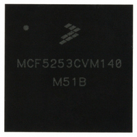
MCF5253CVM140 Freescale Semiconductor, MCF5253CVM140 Datasheet - Page 170

MCF5253CVM140
Manufacturer Part Number
MCF5253CVM140
Description
IC MPU 32BIT 140MHZ 225-MAPBGA
Manufacturer
Freescale Semiconductor
Series
MCF525xr
Datasheets
1.MCF5253VM140J.pdf
(34 pages)
2.MCF5253VM140J.pdf
(8 pages)
3.MCF5253VM140J.pdf
(648 pages)
4.MCF5253VM140J.pdf
(2 pages)
Specifications of MCF5253CVM140
Core Processor
Coldfire V2
Core Size
32-Bit
Speed
140MHz
Connectivity
CAN, EBI/EMI, I²C, QSPI, UART/USART, USB OTG
Peripherals
DMA, WDT
Program Memory Type
ROMless
Ram Size
128K x 8
Voltage - Supply (vcc/vdd)
1.08 V ~ 1.32 V
Data Converters
A/D 6x12b
Oscillator Type
External
Operating Temperature
-40°C ~ 85°C
Package / Case
225-MAPBGA
Family Name
MCF5xxx
Device Core
ColdFire V2
Device Core Size
32b
Frequency (max)
140MHz
Instruction Set Architecture
RISC
Supply Voltage 1 (typ)
1.2/3.3V
Operating Supply Voltage (max)
1.32/3.6V
Operating Supply Voltage (min)
1.08/3V
Operating Temp Range
-40C to 85C
Operating Temperature Classification
Industrial
Mounting
Surface Mount
Pin Count
225
Package Type
MA-BGA
Lead Free Status / RoHS Status
Lead free / RoHS Compliant
Number Of I /o
-
Eeprom Size
-
Program Memory Size
-
Lead Free Status / Rohs Status
Compliant
Available stocks
Company
Part Number
Manufacturer
Quantity
Price
Company:
Part Number:
MCF5253CVM140
Manufacturer:
FREESCALE
Quantity:
300
Company:
Part Number:
MCF5253CVM140
Manufacturer:
Freescale Semiconductor
Quantity:
10 000
Part Number:
MCF5253CVM140
Manufacturer:
FREESCALE
Quantity:
20 000
Company:
Part Number:
MCF5253CVM140J
Manufacturer:
Freescale Semiconductor
Quantity:
10 000
- MCF5253VM140J PDF datasheet
- MCF5253VM140J PDF datasheet #2
- MCF5253VM140J PDF datasheet #3
- MCF5253VM140J PDF datasheet #4
- Current page: 170 of 648
- Download datasheet (8Mb)
System Integration Module (SIM)
9.8.1.1
There are seven general purpose inputs, those associated with GPIO-READ(6:0), have interrupt capability.
On every low-to-high edge transition of these inputs, one of the bits 0–6 of register GPIO-INT-STAT is
set. On every high-to-low edge of the inputs, one of the bits 8–14 is set. Write 1 to clear to the
corresponding bit in GPIO-INT-CLEAR register. If any bit in GPIO-INT-STAT is set, and the
corresponding bit in GPIO-INT-EN is set, an interrupt will be made pending on the secondary interrupt
controller.
Set the GPIO_FUNCTION register bit to 1 or 0 for interrupts, as applicable.
9-26
GPIO-READ(5)
GPIO-READ(4)
GPIO-READ(3)
GPIO-READ(2)
GPIO-READ(1)
GPIO-READ(0)
Purpose Input
General
General Purpose Input Interrupts
MCLK1 will output a clock signal just after reset and before it can be
configured as a GPIO if so desired. The frequency of the clock will be the
same as CRIN prior to initialization of the PLL.
EBUOUT1 will output a clock signal just after reset and before they can be
configured as GPIO. The frequency of the clock output will be CRIN/16.
These two pins can still be used for GPIO. The user needs to ensure that
when one of these two pins is assigned as a GPIO control within the system,
that its use will not cause the application to exhibit problems when the clock
is active just after reset and before the boot code sets them to GPIO mode,
e.g., do not use these pins to switch a critical circuit on/off.
The registers GPIO-INT-STAT, GPIO-INT-CLEAR and GPIO-INT-EN also
control some audio interrupts.
DDATA0/CTS1/SDATA0_SDIO1/GPIO1
DDATA1/RTS1/SDATA2_BS2/GPIO2
Table 9-27. General Purpose Input to Pin Mapping (continued)
DDATA2/CTSO/GPIO3
DDATA3/RTS0/GPIO4
XTRIM/TXD2/GPIO0
Read From Pin
CFLG/GPIO5
MCF5253 Reference Manual, Rev. 1
NOTE
NOTE
NOTE
General Purpose Input
GPIO1-READ(37)
GPIO1-READ(36)
GPIO1-READ(35)
GPIO1-READ(33)
GPIO1-READ(32)
GPIO1-READ(34)
IDE_IORDY/GPIO33
IDE_DIOW/GPIO32
EBUOUT1/GPIO37
SDATAO2/GPIO34
EBUIN1/GPIO36
Freescale Semiconductor
Read From Pin
SCLK3/GPIO35
Related parts for MCF5253CVM140
Image
Part Number
Description
Manufacturer
Datasheet
Request
R
Part Number:
Description:
Mcf5253 Coldfire? Microprocessor Data Sheet
Manufacturer:
Freescale Semiconductor, Inc
Datasheet:
Part Number:
Description:
Manufacturer:
Freescale Semiconductor, Inc
Datasheet:
Part Number:
Description:
Manufacturer:
Freescale Semiconductor, Inc
Datasheet:
Part Number:
Description:
Manufacturer:
Freescale Semiconductor, Inc
Datasheet:
Part Number:
Description:
Manufacturer:
Freescale Semiconductor, Inc
Datasheet:
Part Number:
Description:
Manufacturer:
Freescale Semiconductor, Inc
Datasheet:
Part Number:
Description:
Manufacturer:
Freescale Semiconductor, Inc
Datasheet:
Part Number:
Description:
Manufacturer:
Freescale Semiconductor, Inc
Datasheet:
Part Number:
Description:
Manufacturer:
Freescale Semiconductor, Inc
Datasheet:
Part Number:
Description:
Manufacturer:
Freescale Semiconductor, Inc
Datasheet:
Part Number:
Description:
Manufacturer:
Freescale Semiconductor, Inc
Datasheet:
Part Number:
Description:
Manufacturer:
Freescale Semiconductor, Inc
Datasheet:
Part Number:
Description:
Manufacturer:
Freescale Semiconductor, Inc
Datasheet:
Part Number:
Description:
Manufacturer:
Freescale Semiconductor, Inc
Datasheet:
Part Number:
Description:
Manufacturer:
Freescale Semiconductor, Inc
Datasheet:


