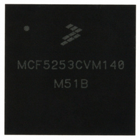
MCF5253CVM140 Freescale Semiconductor, MCF5253CVM140 Datasheet - Page 211

MCF5253CVM140
Manufacturer Part Number
MCF5253CVM140
Description
IC MPU 32BIT 140MHZ 225-MAPBGA
Manufacturer
Freescale Semiconductor
Series
MCF525xr
Datasheets
1.MCF5253VM140J.pdf
(34 pages)
2.MCF5253VM140J.pdf
(8 pages)
3.MCF5253VM140J.pdf
(648 pages)
4.MCF5253VM140J.pdf
(2 pages)
Specifications of MCF5253CVM140
Core Processor
Coldfire V2
Core Size
32-Bit
Speed
140MHz
Connectivity
CAN, EBI/EMI, I²C, QSPI, UART/USART, USB OTG
Peripherals
DMA, WDT
Program Memory Type
ROMless
Ram Size
128K x 8
Voltage - Supply (vcc/vdd)
1.08 V ~ 1.32 V
Data Converters
A/D 6x12b
Oscillator Type
External
Operating Temperature
-40°C ~ 85°C
Package / Case
225-MAPBGA
Family Name
MCF5xxx
Device Core
ColdFire V2
Device Core Size
32b
Frequency (max)
140MHz
Instruction Set Architecture
RISC
Supply Voltage 1 (typ)
1.2/3.3V
Operating Supply Voltage (max)
1.32/3.6V
Operating Supply Voltage (min)
1.08/3V
Operating Temp Range
-40C to 85C
Operating Temperature Classification
Industrial
Mounting
Surface Mount
Pin Count
225
Package Type
MA-BGA
Lead Free Status / RoHS Status
Lead free / RoHS Compliant
Number Of I /o
-
Eeprom Size
-
Program Memory Size
-
Lead Free Status / Rohs Status
Compliant
Available stocks
Company
Part Number
Manufacturer
Quantity
Price
Company:
Part Number:
MCF5253CVM140
Manufacturer:
FREESCALE
Quantity:
300
Company:
Part Number:
MCF5253CVM140
Manufacturer:
Freescale Semiconductor
Quantity:
10 000
Part Number:
MCF5253CVM140
Manufacturer:
FREESCALE
Quantity:
20 000
Company:
Part Number:
MCF5253CVM140J
Manufacturer:
Freescale Semiconductor
Quantity:
10 000
- MCF5253VM140J PDF datasheet
- MCF5253VM140J PDF datasheet #2
- MCF5253VM140J PDF datasheet #3
- MCF5253VM140J PDF datasheet #4
- Current page: 211 of 648
- Download datasheet (8Mb)
1
2
3
13.5.2
The Flash Media interface is built around two Interface Shift Registers, each of which work independently.
Figure 13-10
Freescale Semiconductor
CLOCKCOUNT1
CLOCKCOUNT0
RECEIVEEDGE
STOPCLOCK
In SD mode, this bit should be programmed 1. In MemoryStick mode, programming 1 gives more relaxed timing, however
Memory Stick specs stipulate it should be 0.
The clock generator will increase the length of some SCLKOUT clock cycles to avoid bus contention when the SDIO pin
switches from input to output, or from output to input mode. The clock generator will stop the SCLKOUT clock if this is
necessary to avoid buffer overrun or buffer underrun.
It is acceptable to reprogram these bits while the interface is running. No glitch will occur on sclk_out.
CARDTYPE
31–22
21–20
17–16
Field
15–8
7–0
19
18
Flash Media Interface Operation
shows a block diagram of one interface shift register.
Reserved
Card Type
00 Sony Memory Stick
01 SecureDigital, 1-bit serial data
11 SecureDigital, 4-bit serial data
Receive Edge
1 Receive data on falling edge of SCLKOUT pin
0 Receive data on rising edge of SCLKOUT pin
Reserved
Stop Clock
00 Normal operation
01 Freeze clock low
10 Freeze clock high
CLOCKCOUNT1+1
CLOCKCOUNT0+1
storeRcvShiftReg
TxBufferEmpty
loadTxShiftReg
Table 13-9. Flash Media Configuration Register Field Descriptions
CommandBits
RcvBufferFull
RxBufferFull
bitCounter
shift_busy
crc_is_0
int_level
3
1
2, 3
2, 3
is the sclk_out_pin high period in number of bus clocks
is the sclk_out_pin low period in number of bus clocks
MCF5253 Reference Manual, Rev. 1
Figure 13-10. Shift Register
stopclock
(to clock generator)
Interface
Shift
Register
Description
BS (MemoryStick mode only)
Serial data
IDE and Flash Media Interface
Res
01
15
15
–
0
0
0
13-13
Related parts for MCF5253CVM140
Image
Part Number
Description
Manufacturer
Datasheet
Request
R
Part Number:
Description:
Mcf5253 Coldfire? Microprocessor Data Sheet
Manufacturer:
Freescale Semiconductor, Inc
Datasheet:
Part Number:
Description:
Manufacturer:
Freescale Semiconductor, Inc
Datasheet:
Part Number:
Description:
Manufacturer:
Freescale Semiconductor, Inc
Datasheet:
Part Number:
Description:
Manufacturer:
Freescale Semiconductor, Inc
Datasheet:
Part Number:
Description:
Manufacturer:
Freescale Semiconductor, Inc
Datasheet:
Part Number:
Description:
Manufacturer:
Freescale Semiconductor, Inc
Datasheet:
Part Number:
Description:
Manufacturer:
Freescale Semiconductor, Inc
Datasheet:
Part Number:
Description:
Manufacturer:
Freescale Semiconductor, Inc
Datasheet:
Part Number:
Description:
Manufacturer:
Freescale Semiconductor, Inc
Datasheet:
Part Number:
Description:
Manufacturer:
Freescale Semiconductor, Inc
Datasheet:
Part Number:
Description:
Manufacturer:
Freescale Semiconductor, Inc
Datasheet:
Part Number:
Description:
Manufacturer:
Freescale Semiconductor, Inc
Datasheet:
Part Number:
Description:
Manufacturer:
Freescale Semiconductor, Inc
Datasheet:
Part Number:
Description:
Manufacturer:
Freescale Semiconductor, Inc
Datasheet:
Part Number:
Description:
Manufacturer:
Freescale Semiconductor, Inc
Datasheet:


