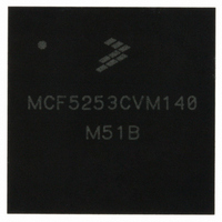
MCF5253CVM140 Freescale Semiconductor, MCF5253CVM140 Datasheet - Page 265

MCF5253CVM140
Manufacturer Part Number
MCF5253CVM140
Description
IC MPU 32BIT 140MHZ 225-MAPBGA
Manufacturer
Freescale Semiconductor
Series
MCF525xr
Datasheets
1.MCF5253VM140J.pdf
(34 pages)
2.MCF5253VM140J.pdf
(8 pages)
3.MCF5253VM140J.pdf
(648 pages)
4.MCF5253VM140J.pdf
(2 pages)
Specifications of MCF5253CVM140
Core Processor
Coldfire V2
Core Size
32-Bit
Speed
140MHz
Connectivity
CAN, EBI/EMI, I²C, QSPI, UART/USART, USB OTG
Peripherals
DMA, WDT
Program Memory Type
ROMless
Ram Size
128K x 8
Voltage - Supply (vcc/vdd)
1.08 V ~ 1.32 V
Data Converters
A/D 6x12b
Oscillator Type
External
Operating Temperature
-40°C ~ 85°C
Package / Case
225-MAPBGA
Family Name
MCF5xxx
Device Core
ColdFire V2
Device Core Size
32b
Frequency (max)
140MHz
Instruction Set Architecture
RISC
Supply Voltage 1 (typ)
1.2/3.3V
Operating Supply Voltage (max)
1.32/3.6V
Operating Supply Voltage (min)
1.08/3V
Operating Temp Range
-40C to 85C
Operating Temperature Classification
Industrial
Mounting
Surface Mount
Pin Count
225
Package Type
MA-BGA
Lead Free Status / RoHS Status
Lead free / RoHS Compliant
Number Of I /o
-
Eeprom Size
-
Program Memory Size
-
Lead Free Status / Rohs Status
Compliant
Available stocks
Company
Part Number
Manufacturer
Quantity
Price
Company:
Part Number:
MCF5253CVM140
Manufacturer:
FREESCALE
Quantity:
300
Company:
Part Number:
MCF5253CVM140
Manufacturer:
Freescale Semiconductor
Quantity:
10 000
Part Number:
MCF5253CVM140
Manufacturer:
FREESCALE
Quantity:
20 000
Company:
Part Number:
MCF5253CVM140J
Manufacturer:
Freescale Semiconductor
Quantity:
10 000
- MCF5253VM140J PDF datasheet
- MCF5253VM140J PDF datasheet #2
- MCF5253VM140J PDF datasheet #3
- MCF5253VM140J PDF datasheet #4
- Current page: 265 of 648
- Download datasheet (8Mb)
15.4.4
To use the timer mode for either the receiver and transmitter channel, program the UCSR registers to the
value $DD.
The transmitter and receiver can be programmed to different clock sources.
Freescale Semiconductor
RCS3–RCS0
TCS3–TCS0
RxRDY
FFULL
Field
1
0
Field
Address MBAR + $1C4 (USCR0
7–4
3–0
Reset
W
R
Receiver Ready
1 One or more characters have been received and are waiting in the receiver buffer FIFO.
0 The CPU has read the receiver buffer and no characters remain in the FIFO after this read.
FIFO Full
1 Three characters have been received and are waiting in the receiver buffer FIFO.
0 The FIFO is not full but can contain as many as two unread characters.
Clock-Select Registers (USCRn)
MBAR + $204 (USCR1)
MBAR2 + $C04 (USCR2)
The Receiver Clock Select bits select the clock source for the receiver channel.
bits necessary for each mode.
The Transmitter Clock Select bits determine the clock source of the UART transmitter channel.
External clock input is not available so this register should always be set to
select internal timer mode.
RCS3
7
1
Table 15-7. Status Registers (USRn) Field Descriptions (continued)
Table 15-8. Clock Select Register (UCSRn) Field Descriptions
RCS2
1
6
Figure 15-11. Clock Select Register (UCSRn)
MCF5253 Reference Manual, Rev. 1
RCS1
RCS3
TCS3
0
5
1
1
1
1
1
1
RCS2
TCS2
1
1
1
1
1
1
NOTE
RCS0
Description
4
1
Description
RCS1
TCS1
0
0
0
0
0
0
RCS0
TCS3
TCS0
1
1
1
1
3
1
1
1
reserved
reserved
reserved
reserved
TIMER
TIMER
SET 1
Mode
TCS2
1
2
Table 15-12
Access: User write only
TCS1
0
1
details the register
UART Modules
TCS0
1
0
15-19
Related parts for MCF5253CVM140
Image
Part Number
Description
Manufacturer
Datasheet
Request
R
Part Number:
Description:
Mcf5253 Coldfire? Microprocessor Data Sheet
Manufacturer:
Freescale Semiconductor, Inc
Datasheet:
Part Number:
Description:
Manufacturer:
Freescale Semiconductor, Inc
Datasheet:
Part Number:
Description:
Manufacturer:
Freescale Semiconductor, Inc
Datasheet:
Part Number:
Description:
Manufacturer:
Freescale Semiconductor, Inc
Datasheet:
Part Number:
Description:
Manufacturer:
Freescale Semiconductor, Inc
Datasheet:
Part Number:
Description:
Manufacturer:
Freescale Semiconductor, Inc
Datasheet:
Part Number:
Description:
Manufacturer:
Freescale Semiconductor, Inc
Datasheet:
Part Number:
Description:
Manufacturer:
Freescale Semiconductor, Inc
Datasheet:
Part Number:
Description:
Manufacturer:
Freescale Semiconductor, Inc
Datasheet:
Part Number:
Description:
Manufacturer:
Freescale Semiconductor, Inc
Datasheet:
Part Number:
Description:
Manufacturer:
Freescale Semiconductor, Inc
Datasheet:
Part Number:
Description:
Manufacturer:
Freescale Semiconductor, Inc
Datasheet:
Part Number:
Description:
Manufacturer:
Freescale Semiconductor, Inc
Datasheet:
Part Number:
Description:
Manufacturer:
Freescale Semiconductor, Inc
Datasheet:
Part Number:
Description:
Manufacturer:
Freescale Semiconductor, Inc
Datasheet:


