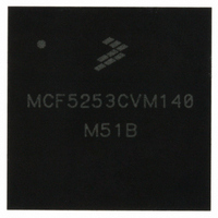
MCF5253CVM140 Freescale Semiconductor, MCF5253CVM140 Datasheet - Page 418

MCF5253CVM140
Manufacturer Part Number
MCF5253CVM140
Description
IC MPU 32BIT 140MHZ 225-MAPBGA
Manufacturer
Freescale Semiconductor
Series
MCF525xr
Datasheets
1.MCF5253VM140J.pdf
(34 pages)
2.MCF5253VM140J.pdf
(8 pages)
3.MCF5253VM140J.pdf
(648 pages)
4.MCF5253VM140J.pdf
(2 pages)
Specifications of MCF5253CVM140
Core Processor
Coldfire V2
Core Size
32-Bit
Speed
140MHz
Connectivity
CAN, EBI/EMI, I²C, QSPI, UART/USART, USB OTG
Peripherals
DMA, WDT
Program Memory Type
ROMless
Ram Size
128K x 8
Voltage - Supply (vcc/vdd)
1.08 V ~ 1.32 V
Data Converters
A/D 6x12b
Oscillator Type
External
Operating Temperature
-40°C ~ 85°C
Package / Case
225-MAPBGA
Family Name
MCF5xxx
Device Core
ColdFire V2
Device Core Size
32b
Frequency (max)
140MHz
Instruction Set Architecture
RISC
Supply Voltage 1 (typ)
1.2/3.3V
Operating Supply Voltage (max)
1.32/3.6V
Operating Supply Voltage (min)
1.08/3V
Operating Temp Range
-40C to 85C
Operating Temperature Classification
Industrial
Mounting
Surface Mount
Pin Count
225
Package Type
MA-BGA
Lead Free Status / RoHS Status
Lead free / RoHS Compliant
Number Of I /o
-
Eeprom Size
-
Program Memory Size
-
Lead Free Status / Rohs Status
Compliant
Available stocks
Company
Part Number
Manufacturer
Quantity
Price
Company:
Part Number:
MCF5253CVM140
Manufacturer:
FREESCALE
Quantity:
300
Company:
Part Number:
MCF5253CVM140
Manufacturer:
Freescale Semiconductor
Quantity:
10 000
Part Number:
MCF5253CVM140
Manufacturer:
FREESCALE
Quantity:
20 000
Company:
Part Number:
MCF5253CVM140J
Manufacturer:
Freescale Semiconductor
Quantity:
10 000
- MCF5253VM140J PDF datasheet
- MCF5253VM140J PDF datasheet #2
- MCF5253VM140J PDF datasheet #3
- MCF5253VM140J PDF datasheet #4
- Current page: 418 of 648
- Download datasheet (8Mb)
IEEE 1149.1 Test Access Port (JTAG)
The HIGHZ instruction goes active on the falling edge of TCK in the update-IR state when the data held
in the instruction shift register is equivalent to 4.
21.5.1.6
The BYPASS instruction selects the single-bit bypass register, creating a single-bit shift register path from
the TDI pin to the bypass register to the TDO pin. This instruction enhances test efficiency by reducing
the overall shift path when a device other than the MCF5253 processor becomes the device under test on
a board design with multiple chips on the overall IEEE1149.1A defined boundary-scan chain. The bypass
register has been implemented in accordance with IEEE1149.1A so that the shift register stage is set to
logic zero on the rising edge of TCK following entry into the capture-DR state. Therefore, the first bit to
be shifted out after selecting the bypass register is always a logic zero (to differentiate a part that supports
an IDCODE register from a part that supports only the bypass register). The BYPASS instruction goes
active on the falling edge of TCK in the update-IR state when the data held in the instruction shift register
is equivalent to 0xF.
21.5.2
An IEEE 1149.1A compliant JTAG identification register has been included on the MCF5253. The
MCF5253 JTAG instruction encoded as 1 provides for reading the JTAG IDcode register.
21-8
31–28 The Version Number bits indicate the revision number of the MCF5253.
27–22 The Design Center bits indicate the Munich design center.
21–12 The Device Number bits indicate an MCF5253.
Address
Field
11–1
0
Reset
Reset
W
W
R
R
The JEDEC ID bits indicate the reduced JEDEC ID for Freescale (JEDEC refers to the Joint Electron Device
Engineering Council. Refer to JEDEC publication 106-A and section 11 of the IEEE 1149.1A Standard for further
information on this field).
Differentiates this register as the JTAG ID code register (as opposed to the bypass register) according to the IEEE
1149.1A Standard.
31
15
0
0
ID Code Register
BYPASS Instruction
VERSION NUMBER
DEVICE NUMBER
30
14
0
1
29
13
1
1
28
12
0
0
Table 21-3. ID Code Register Field Descriptions
Figure 21-3. ID Code Register Command
27
11
0
0
MCF5253 Reference Manual, Rev. 1
26
10
1
0
DESIGN CENTER
25
0
0
9
Description
24
1
0
8
23
0
0
7
JEDECID
22
1
0
6
21
0
0
5
20
0
1
4
DEVICE NUMBER
19
0
1
3
Freescale Semiconductor
Access: User read-only
18
0
2
1
17
0
0
1
JTAGID
16
0
1
0
Related parts for MCF5253CVM140
Image
Part Number
Description
Manufacturer
Datasheet
Request
R
Part Number:
Description:
Mcf5253 Coldfire? Microprocessor Data Sheet
Manufacturer:
Freescale Semiconductor, Inc
Datasheet:
Part Number:
Description:
Manufacturer:
Freescale Semiconductor, Inc
Datasheet:
Part Number:
Description:
Manufacturer:
Freescale Semiconductor, Inc
Datasheet:
Part Number:
Description:
Manufacturer:
Freescale Semiconductor, Inc
Datasheet:
Part Number:
Description:
Manufacturer:
Freescale Semiconductor, Inc
Datasheet:
Part Number:
Description:
Manufacturer:
Freescale Semiconductor, Inc
Datasheet:
Part Number:
Description:
Manufacturer:
Freescale Semiconductor, Inc
Datasheet:
Part Number:
Description:
Manufacturer:
Freescale Semiconductor, Inc
Datasheet:
Part Number:
Description:
Manufacturer:
Freescale Semiconductor, Inc
Datasheet:
Part Number:
Description:
Manufacturer:
Freescale Semiconductor, Inc
Datasheet:
Part Number:
Description:
Manufacturer:
Freescale Semiconductor, Inc
Datasheet:
Part Number:
Description:
Manufacturer:
Freescale Semiconductor, Inc
Datasheet:
Part Number:
Description:
Manufacturer:
Freescale Semiconductor, Inc
Datasheet:
Part Number:
Description:
Manufacturer:
Freescale Semiconductor, Inc
Datasheet:
Part Number:
Description:
Manufacturer:
Freescale Semiconductor, Inc
Datasheet:


