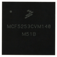
MCF5253CVM140 Freescale Semiconductor, MCF5253CVM140 Datasheet - Page 348

MCF5253CVM140
Manufacturer Part Number
MCF5253CVM140
Description
IC MPU 32BIT 140MHZ 225-MAPBGA
Manufacturer
Freescale Semiconductor
Series
MCF525xr
Datasheets
1.MCF5253VM140J.pdf
(34 pages)
2.MCF5253VM140J.pdf
(8 pages)
3.MCF5253VM140J.pdf
(648 pages)
4.MCF5253VM140J.pdf
(2 pages)
Specifications of MCF5253CVM140
Core Processor
Coldfire V2
Core Size
32-Bit
Speed
140MHz
Connectivity
CAN, EBI/EMI, I²C, QSPI, UART/USART, USB OTG
Peripherals
DMA, WDT
Program Memory Type
ROMless
Ram Size
128K x 8
Voltage - Supply (vcc/vdd)
1.08 V ~ 1.32 V
Data Converters
A/D 6x12b
Oscillator Type
External
Operating Temperature
-40°C ~ 85°C
Package / Case
225-MAPBGA
Family Name
MCF5xxx
Device Core
ColdFire V2
Device Core Size
32b
Frequency (max)
140MHz
Instruction Set Architecture
RISC
Supply Voltage 1 (typ)
1.2/3.3V
Operating Supply Voltage (max)
1.32/3.6V
Operating Supply Voltage (min)
1.08/3V
Operating Temp Range
-40C to 85C
Operating Temperature Classification
Industrial
Mounting
Surface Mount
Pin Count
225
Package Type
MA-BGA
Lead Free Status / RoHS Status
Lead free / RoHS Compliant
Number Of I /o
-
Eeprom Size
-
Program Memory Size
-
Lead Free Status / Rohs Status
Compliant
Available stocks
Company
Part Number
Manufacturer
Quantity
Price
Company:
Part Number:
MCF5253CVM140
Manufacturer:
FREESCALE
Quantity:
300
Company:
Part Number:
MCF5253CVM140
Manufacturer:
Freescale Semiconductor
Quantity:
10 000
Part Number:
MCF5253CVM140
Manufacturer:
FREESCALE
Quantity:
20 000
Company:
Part Number:
MCF5253CVM140J
Manufacturer:
Freescale Semiconductor
Quantity:
10 000
- MCF5253VM140J PDF datasheet
- MCF5253VM140J PDF datasheet #2
- MCF5253VM140J PDF datasheet #3
- MCF5253VM140J PDF datasheet #4
- Current page: 348 of 648
- Download datasheet (8Mb)
I
18.4.1
When the bus is free, for example, no master device is engaging the bus (both SCL and SDA lines are at
logic high), a master can initiate communication by sending a START signal. As shown in
START signal is defined as a high-to-low transition of SDA while SCL is high. This signal denotes the
beginning of a new data transfer (each data transfer can contain several bytes of data) and awakens all
slaves.
18.4.2
The first byte of data transferred by the master immediately after the START signal is the slave address.
This is a seven-bit calling address followed by a R/W bit. The R/W bit tells the slave data transfer direction.
No two slaves in the system can have the same address. In addition, if the I
an address that is equal to its slave address. The I
Only the slave with an address that matches the one transmitted by the master will respond. It returns an
acknowledge bit by pulling the SDA low at the 9th clock (see
18.4.3
Once successful slave addressing is achieved, the data transfer can proceed on a byte-by-byte basis in the
direction specified by the R/W bit sent by the calling master.
18-4
2
C Modules
SCL
SCL
SDA
SDA
START
SIGNAL
START
SIGNAL
START Signal
Slave Address Transmission
Data Transfer
AD7 AD6 AD5 AD4 AD3 AD2 AD1 R/W
AD7 AD6 AD5 AD4 AD3 AD2 AD1 R/W
MSB
MSB
1
1
2
2
CALLING ADDRESS
CALLING ADDRESS
3
3
4
4
Figure 18-2. I
5
5
6
6
MCF5253 Reference Manual, Rev. 1
7
7
R/W ACK
2
R/W
LSB
LSB
C Standard Communication Protocol
8
8
ACK
BIT
BIT
9
9
XX
2
C cannot be master and slave at the same time.
XXX
REPEATED
START
SIGNAL
AD7 AD6 AD5 AD4 AD3 AD2 AD1 R/W
MSB
MSB
D7 D6 D5
1
1
2
2
Figure
STOP
NEW CALLING ADDRESS
3
3
DATA BYTE
D4 D3
4
4
18-2).
5
5
2
C is master, it must not transmit
D2 D1
6
6
7
7
R/W NO
LSB
LSB
D0
Freescale Semiconductor
8
8
NO
ACK
BIT
ACK
BIT
9
9
Figure
STOP
SIGNAL
STOP
SIGNAL
18-2, a
Related parts for MCF5253CVM140
Image
Part Number
Description
Manufacturer
Datasheet
Request
R
Part Number:
Description:
Mcf5253 Coldfire? Microprocessor Data Sheet
Manufacturer:
Freescale Semiconductor, Inc
Datasheet:
Part Number:
Description:
Manufacturer:
Freescale Semiconductor, Inc
Datasheet:
Part Number:
Description:
Manufacturer:
Freescale Semiconductor, Inc
Datasheet:
Part Number:
Description:
Manufacturer:
Freescale Semiconductor, Inc
Datasheet:
Part Number:
Description:
Manufacturer:
Freescale Semiconductor, Inc
Datasheet:
Part Number:
Description:
Manufacturer:
Freescale Semiconductor, Inc
Datasheet:
Part Number:
Description:
Manufacturer:
Freescale Semiconductor, Inc
Datasheet:
Part Number:
Description:
Manufacturer:
Freescale Semiconductor, Inc
Datasheet:
Part Number:
Description:
Manufacturer:
Freescale Semiconductor, Inc
Datasheet:
Part Number:
Description:
Manufacturer:
Freescale Semiconductor, Inc
Datasheet:
Part Number:
Description:
Manufacturer:
Freescale Semiconductor, Inc
Datasheet:
Part Number:
Description:
Manufacturer:
Freescale Semiconductor, Inc
Datasheet:
Part Number:
Description:
Manufacturer:
Freescale Semiconductor, Inc
Datasheet:
Part Number:
Description:
Manufacturer:
Freescale Semiconductor, Inc
Datasheet:
Part Number:
Description:
Manufacturer:
Freescale Semiconductor, Inc
Datasheet:


