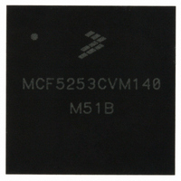
MCF5253CVM140 Freescale Semiconductor, MCF5253CVM140 Datasheet - Page 106

MCF5253CVM140
Manufacturer Part Number
MCF5253CVM140
Description
IC MPU 32BIT 140MHZ 225-MAPBGA
Manufacturer
Freescale Semiconductor
Series
MCF525xr
Datasheets
1.MCF5253VM140J.pdf
(34 pages)
2.MCF5253VM140J.pdf
(8 pages)
3.MCF5253VM140J.pdf
(648 pages)
4.MCF5253VM140J.pdf
(2 pages)
Specifications of MCF5253CVM140
Core Processor
Coldfire V2
Core Size
32-Bit
Speed
140MHz
Connectivity
CAN, EBI/EMI, I²C, QSPI, UART/USART, USB OTG
Peripherals
DMA, WDT
Program Memory Type
ROMless
Ram Size
128K x 8
Voltage - Supply (vcc/vdd)
1.08 V ~ 1.32 V
Data Converters
A/D 6x12b
Oscillator Type
External
Operating Temperature
-40°C ~ 85°C
Package / Case
225-MAPBGA
Family Name
MCF5xxx
Device Core
ColdFire V2
Device Core Size
32b
Frequency (max)
140MHz
Instruction Set Architecture
RISC
Supply Voltage 1 (typ)
1.2/3.3V
Operating Supply Voltage (max)
1.32/3.6V
Operating Supply Voltage (min)
1.08/3V
Operating Temp Range
-40C to 85C
Operating Temperature Classification
Industrial
Mounting
Surface Mount
Pin Count
225
Package Type
MA-BGA
Lead Free Status / RoHS Status
Lead free / RoHS Compliant
Number Of I /o
-
Eeprom Size
-
Program Memory Size
-
Lead Free Status / Rohs Status
Compliant
Available stocks
Company
Part Number
Manufacturer
Quantity
Price
Company:
Part Number:
MCF5253CVM140
Manufacturer:
FREESCALE
Quantity:
300
Company:
Part Number:
MCF5253CVM140
Manufacturer:
Freescale Semiconductor
Quantity:
10 000
Part Number:
MCF5253CVM140
Manufacturer:
FREESCALE
Quantity:
20 000
Company:
Part Number:
MCF5253CVM140J
Manufacturer:
Freescale Semiconductor
Quantity:
10 000
- MCF5253VM140J PDF datasheet
- MCF5253VM140J PDF datasheet #2
- MCF5253VM140J PDF datasheet #3
- MCF5253VM140J PDF datasheet #4
- Current page: 106 of 648
- Download datasheet (8Mb)
Synchronous DRAM Controller Module
The DRAM controller’s major components, shown in
7.2
By running synchronously with the system clock, the SDRAM can (after an initial latency period) be
accessed on every clock; 5-1-1-1 is a typical MCF5253 burst rate to SDRAM.
Table 7-1
7-2
Command
SELFX
WRITE
READ
ACTV
SELF
MRS
PALL
NOP
REF
•
•
•
•
•
DRAM address and control register (DACR0)—The DRAM controller consists of a configuration
register unit. DACR0 is accessed at MBAR + 0x0108;
The register information is passed on to the hit logic.
Control logic and state machine—Generates all DRAM signals, taking bus cycle characteristic data
from the block logic, along with hit information to generate DRAM accesses. Handles refresh
requests from the refresh counter.
— DRAM control register (DCR)—Contains data to control refresh operation of the DRAM
— Refresh counter—Determines when refresh should occur, determined by the value of
Hit logic—Compares address and attribute signals of a current DRAM bus cycle to DACR to
determine if the DRAM block is being accessed. Hits are passed to the control logic along with
characteristics of the bus cycle to be generated.
Page hit logic—Determines if the next DRAM access is in the same DRAM page as the previous
one. This information is passed on to the control logic.
Address multiplexing—Multiplexes addresses to allow column and row addresses to share pins.
This allows glueless interface to DRAMs.
Synchronous Operation
lists common SDRAM commands.
Activate. Executed before
Mode register set.
No-op. Does not affect SDRAM state machine; DRAM controller control signals negated; SD_CS0 asserted.
Precharge all. Precharges all internal banks of an SDRAM component; executed before new page is opened.
Read access. SDRAM registers column address and decodes that a read access is occurring.
Refresh. Refreshes internal bank rows of SDRAM.
Self refresh. Refreshes internal bank rows of SDRAM when it is in low-power mode.
Exit self refresh. This command is sent to the DRAM controller when DCR[IS] is cleared.
Write access.
controller. The memory block is refreshed concurrently as controlled by DCR[RC].
DCR[RC]. It generates a refresh request to the control block.
Because the MCF5253 cannot have more than one page open at a time, it
does not support interleaving.
READ
MCF5253 Reference Manual, Rev. 1
or
Table 7-1. SDRAM Commands
WRITE
executes; SDRAM registers and decodes row address.
NOTE
Definition
Figure
7-1, are described as follows:
Freescale Semiconductor
Related parts for MCF5253CVM140
Image
Part Number
Description
Manufacturer
Datasheet
Request
R
Part Number:
Description:
Mcf5253 Coldfire? Microprocessor Data Sheet
Manufacturer:
Freescale Semiconductor, Inc
Datasheet:
Part Number:
Description:
Manufacturer:
Freescale Semiconductor, Inc
Datasheet:
Part Number:
Description:
Manufacturer:
Freescale Semiconductor, Inc
Datasheet:
Part Number:
Description:
Manufacturer:
Freescale Semiconductor, Inc
Datasheet:
Part Number:
Description:
Manufacturer:
Freescale Semiconductor, Inc
Datasheet:
Part Number:
Description:
Manufacturer:
Freescale Semiconductor, Inc
Datasheet:
Part Number:
Description:
Manufacturer:
Freescale Semiconductor, Inc
Datasheet:
Part Number:
Description:
Manufacturer:
Freescale Semiconductor, Inc
Datasheet:
Part Number:
Description:
Manufacturer:
Freescale Semiconductor, Inc
Datasheet:
Part Number:
Description:
Manufacturer:
Freescale Semiconductor, Inc
Datasheet:
Part Number:
Description:
Manufacturer:
Freescale Semiconductor, Inc
Datasheet:
Part Number:
Description:
Manufacturer:
Freescale Semiconductor, Inc
Datasheet:
Part Number:
Description:
Manufacturer:
Freescale Semiconductor, Inc
Datasheet:
Part Number:
Description:
Manufacturer:
Freescale Semiconductor, Inc
Datasheet:
Part Number:
Description:
Manufacturer:
Freescale Semiconductor, Inc
Datasheet:


