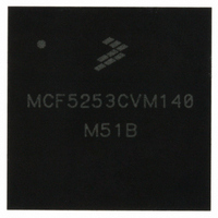
MCF5253CVM140 Freescale Semiconductor, MCF5253CVM140 Datasheet - Page 244

MCF5253CVM140
Manufacturer Part Number
MCF5253CVM140
Description
IC MPU 32BIT 140MHZ 225-MAPBGA
Manufacturer
Freescale Semiconductor
Series
MCF525xr
Datasheets
1.MCF5253VM140J.pdf
(34 pages)
2.MCF5253VM140J.pdf
(8 pages)
3.MCF5253VM140J.pdf
(648 pages)
4.MCF5253VM140J.pdf
(2 pages)
Specifications of MCF5253CVM140
Core Processor
Coldfire V2
Core Size
32-Bit
Speed
140MHz
Connectivity
CAN, EBI/EMI, I²C, QSPI, UART/USART, USB OTG
Peripherals
DMA, WDT
Program Memory Type
ROMless
Ram Size
128K x 8
Voltage - Supply (vcc/vdd)
1.08 V ~ 1.32 V
Data Converters
A/D 6x12b
Oscillator Type
External
Operating Temperature
-40°C ~ 85°C
Package / Case
225-MAPBGA
Family Name
MCF5xxx
Device Core
ColdFire V2
Device Core Size
32b
Frequency (max)
140MHz
Instruction Set Architecture
RISC
Supply Voltage 1 (typ)
1.2/3.3V
Operating Supply Voltage (max)
1.32/3.6V
Operating Supply Voltage (min)
1.08/3V
Operating Temp Range
-40C to 85C
Operating Temperature Classification
Industrial
Mounting
Surface Mount
Pin Count
225
Package Type
MA-BGA
Lead Free Status / RoHS Status
Lead free / RoHS Compliant
Number Of I /o
-
Eeprom Size
-
Program Memory Size
-
Lead Free Status / Rohs Status
Compliant
Available stocks
Company
Part Number
Manufacturer
Quantity
Price
Company:
Part Number:
MCF5253CVM140
Manufacturer:
FREESCALE
Quantity:
300
Company:
Part Number:
MCF5253CVM140
Manufacturer:
Freescale Semiconductor
Quantity:
10 000
Part Number:
MCF5253CVM140
Manufacturer:
FREESCALE
Quantity:
20 000
Company:
Part Number:
MCF5253CVM140J
Manufacturer:
Freescale Semiconductor
Quantity:
10 000
- MCF5253VM140J PDF datasheet
- MCF5253VM140J PDF datasheet #2
- MCF5253VM140J PDF datasheet #3
- MCF5253VM140J PDF datasheet #4
- Current page: 244 of 648
- Download datasheet (8Mb)
DMA Controller
14.7.2
14.7.2.1
All channels can initiate transfers to/from a periphery module by means of REQUEST[3:0]. Source where
REQUEST is coming from is programmed in register DMAROUTE. If the EEXT bit (DCR[30]) is set,
when a REQUEST is asserted, the DMA initiates a transfer provided the channel is idle. If the CS (cycle
steal) bit is set, the read/write transaction on the bus is limited to a single transfer. If the CS bit is clear,
multiple read/write transfers can occur on the bus as programmed. REQUEST does not need to be negated
until the DONE bit (DSR[0]) is set.
14.7.2.2
This feature allows for block transfers to occur at the optimum size based on the address, byte count, and
programmed size. To use this feature, AA in the DCR must be set. The source is auto-aligned when the
SSIZE bits indicate a larger transfer size compared to DSIZE. Source alignment takes precedence over the
destination when the source and destination sizes are equal. Otherwise, the destination is auto-aligned. The
address register that is chosen for alignment increments regardless of the value of the increment bit.
Configuration error checking is performed on the registers that are not chosen for alignment.
If the BCR contains a value greater than 16, the address will determine the size of the transfer. Single byte,
word or longword transfers will occur until the address is aligned to the programmed size boundary, at
which time the programmed size accesses begin. When the BCR is less than 16 at the beginning of a
read/write transfer, the number of bytes remaining will dictate the transfer size, longword, word or byte.
For example:
Because the SSIZE > DSIZE, the source is auto-aligned. Error checking is performed on the destination
registers. The sequence of accesses is as follows:
If DSIZE is set to another size, then the data writes are optimized to write the largest size allowed based
on the address, but not exceeding the configured size.
14.7.2.3
This feature makes provision to force the DMA off the bus to allow another master access. Bus arbiter
design was simplified by making arbitration programmable. The decode of the DCR[BWC] field provides
7 levels of block transfer sizes. If the BCR decrements to a value that is a multiple of the decode of the
BWC, the DMA bus request negates until termination of the bus cycle. Should a request be pending, the
arbiter may then choose to switch the bus to another master. If auto-alignment is enabled (DCR[AA] = 1),
14-16
1. Read byte from $0001—write byte, increment SAR
2. Read word from $0002—write 2 bytes, increment SAR
3. Read long word from $0004—write 4 bytes, increment SAR
4. Repeat longwords until SAR = $00f0
5. Read byte from $00f0—write byte, increment SAR.
AA = 1, SAR = $0001, BCR = $00f0, SSIZE = 00 (longword) and DSIZE = 01 (byte),
Data Transfer
Periphery Request Operation
Auto Alignment
Bandwidth Control
MCF5253 Reference Manual, Rev. 1
Freescale Semiconductor
Related parts for MCF5253CVM140
Image
Part Number
Description
Manufacturer
Datasheet
Request
R
Part Number:
Description:
Mcf5253 Coldfire? Microprocessor Data Sheet
Manufacturer:
Freescale Semiconductor, Inc
Datasheet:
Part Number:
Description:
Manufacturer:
Freescale Semiconductor, Inc
Datasheet:
Part Number:
Description:
Manufacturer:
Freescale Semiconductor, Inc
Datasheet:
Part Number:
Description:
Manufacturer:
Freescale Semiconductor, Inc
Datasheet:
Part Number:
Description:
Manufacturer:
Freescale Semiconductor, Inc
Datasheet:
Part Number:
Description:
Manufacturer:
Freescale Semiconductor, Inc
Datasheet:
Part Number:
Description:
Manufacturer:
Freescale Semiconductor, Inc
Datasheet:
Part Number:
Description:
Manufacturer:
Freescale Semiconductor, Inc
Datasheet:
Part Number:
Description:
Manufacturer:
Freescale Semiconductor, Inc
Datasheet:
Part Number:
Description:
Manufacturer:
Freescale Semiconductor, Inc
Datasheet:
Part Number:
Description:
Manufacturer:
Freescale Semiconductor, Inc
Datasheet:
Part Number:
Description:
Manufacturer:
Freescale Semiconductor, Inc
Datasheet:
Part Number:
Description:
Manufacturer:
Freescale Semiconductor, Inc
Datasheet:
Part Number:
Description:
Manufacturer:
Freescale Semiconductor, Inc
Datasheet:
Part Number:
Description:
Manufacturer:
Freescale Semiconductor, Inc
Datasheet:


