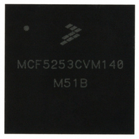
MCF5253CVM140 Freescale Semiconductor, MCF5253CVM140 Datasheet - Page 124

MCF5253CVM140
Manufacturer Part Number
MCF5253CVM140
Description
IC MPU 32BIT 140MHZ 225-MAPBGA
Manufacturer
Freescale Semiconductor
Series
MCF525xr
Datasheets
1.MCF5253VM140J.pdf
(34 pages)
2.MCF5253VM140J.pdf
(8 pages)
3.MCF5253VM140J.pdf
(648 pages)
4.MCF5253VM140J.pdf
(2 pages)
Specifications of MCF5253CVM140
Core Processor
Coldfire V2
Core Size
32-Bit
Speed
140MHz
Connectivity
CAN, EBI/EMI, I²C, QSPI, UART/USART, USB OTG
Peripherals
DMA, WDT
Program Memory Type
ROMless
Ram Size
128K x 8
Voltage - Supply (vcc/vdd)
1.08 V ~ 1.32 V
Data Converters
A/D 6x12b
Oscillator Type
External
Operating Temperature
-40°C ~ 85°C
Package / Case
225-MAPBGA
Family Name
MCF5xxx
Device Core
ColdFire V2
Device Core Size
32b
Frequency (max)
140MHz
Instruction Set Architecture
RISC
Supply Voltage 1 (typ)
1.2/3.3V
Operating Supply Voltage (max)
1.32/3.6V
Operating Supply Voltage (min)
1.08/3V
Operating Temp Range
-40C to 85C
Operating Temperature Classification
Industrial
Mounting
Surface Mount
Pin Count
225
Package Type
MA-BGA
Lead Free Status / RoHS Status
Lead free / RoHS Compliant
Number Of I /o
-
Eeprom Size
-
Program Memory Size
-
Lead Free Status / Rohs Status
Compliant
Available stocks
Company
Part Number
Manufacturer
Quantity
Price
Company:
Part Number:
MCF5253CVM140
Manufacturer:
FREESCALE
Quantity:
300
Company:
Part Number:
MCF5253CVM140
Manufacturer:
Freescale Semiconductor
Quantity:
10 000
Part Number:
MCF5253CVM140
Manufacturer:
FREESCALE
Quantity:
20 000
Company:
Part Number:
MCF5253CVM140J
Manufacturer:
Freescale Semiconductor
Quantity:
10 000
- MCF5253VM140J PDF datasheet
- MCF5253VM140J PDF datasheet #2
- MCF5253VM140J PDF datasheet #3
- MCF5253VM140J PDF datasheet #4
- Current page: 124 of 648
- Download datasheet (8Mb)
Synchronous DRAM Controller Module
7.6.4
In this example, only the second 512 Kbyte block of each 1 Mbyte space is accessed in each bank. In
addition the SDRAM component is mapped only to readable and writable supervisor and user data. The
DMRs have the following configuration.
With this configuration, the DMR0 = 0x0074_0075, as described in
7-20
31–16
IMRS
BAM
15–9
Field Setting
Bits
WP
5–4
1–0
PM
PS
IP
Setting
Setting
8
7
7
6
3
2
(hex)
(hex)
Field
Field
Setting
10
–
–
0
–
–
0
0
1
–
31
15
0
–
DMR Initialization
With bits 17 and 16 as don’t cares, BAM = 0x0074, which leaves bank select bits and upper 512K select bits
unmasked.
Bits 22 and 21 are set because they are used as bank selects; bit 20 is set because it controls the 1-MB
boundary address.
Reserved. Don’t care.
Allow reads and writes
Reserved
Reserved. Don’t care.
Indicates
16-bit port.
Indicates precharge has not been initiated.
Indicates continuous page mode.
Reserved. Don’t care.
30
14
0
–
0
0
MRS
29
13
0
–
command has not been initiated.
Table 7-15. DACR Initialization Values (continued)
28
12
0
–
Table 7-16. DMR0 Initialization Values
27
11
0
–
MCF5253 Reference Manual, Rev. 1
Figure 7-16. DMR0 Register
26
10
0
–
0
0
25
0
–
9
BAM
WP
24
0
0
8
Description
Description
23
0
–
7
C/I
22
1
1
6
Table
7
7
AM
21
1
1
5
7-16.
SC
20
1
1
4
SD
19
0
0
3
Freescale Semiconductor
UC
18
1
1
2
4
5
UD
17
–
0
1
16
V
–
1
0
Related parts for MCF5253CVM140
Image
Part Number
Description
Manufacturer
Datasheet
Request
R
Part Number:
Description:
Mcf5253 Coldfire? Microprocessor Data Sheet
Manufacturer:
Freescale Semiconductor, Inc
Datasheet:
Part Number:
Description:
Manufacturer:
Freescale Semiconductor, Inc
Datasheet:
Part Number:
Description:
Manufacturer:
Freescale Semiconductor, Inc
Datasheet:
Part Number:
Description:
Manufacturer:
Freescale Semiconductor, Inc
Datasheet:
Part Number:
Description:
Manufacturer:
Freescale Semiconductor, Inc
Datasheet:
Part Number:
Description:
Manufacturer:
Freescale Semiconductor, Inc
Datasheet:
Part Number:
Description:
Manufacturer:
Freescale Semiconductor, Inc
Datasheet:
Part Number:
Description:
Manufacturer:
Freescale Semiconductor, Inc
Datasheet:
Part Number:
Description:
Manufacturer:
Freescale Semiconductor, Inc
Datasheet:
Part Number:
Description:
Manufacturer:
Freescale Semiconductor, Inc
Datasheet:
Part Number:
Description:
Manufacturer:
Freescale Semiconductor, Inc
Datasheet:
Part Number:
Description:
Manufacturer:
Freescale Semiconductor, Inc
Datasheet:
Part Number:
Description:
Manufacturer:
Freescale Semiconductor, Inc
Datasheet:
Part Number:
Description:
Manufacturer:
Freescale Semiconductor, Inc
Datasheet:
Part Number:
Description:
Manufacturer:
Freescale Semiconductor, Inc
Datasheet:


