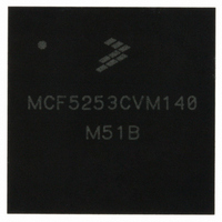
MCF5253CVM140 Freescale Semiconductor, MCF5253CVM140 Datasheet - Page 398

MCF5253CVM140
Manufacturer Part Number
MCF5253CVM140
Description
IC MPU 32BIT 140MHZ 225-MAPBGA
Manufacturer
Freescale Semiconductor
Series
MCF525xr
Datasheets
1.MCF5253VM140J.pdf
(34 pages)
2.MCF5253VM140J.pdf
(8 pages)
3.MCF5253VM140J.pdf
(648 pages)
4.MCF5253VM140J.pdf
(2 pages)
Specifications of MCF5253CVM140
Core Processor
Coldfire V2
Core Size
32-Bit
Speed
140MHz
Connectivity
CAN, EBI/EMI, I²C, QSPI, UART/USART, USB OTG
Peripherals
DMA, WDT
Program Memory Type
ROMless
Ram Size
128K x 8
Voltage - Supply (vcc/vdd)
1.08 V ~ 1.32 V
Data Converters
A/D 6x12b
Oscillator Type
External
Operating Temperature
-40°C ~ 85°C
Package / Case
225-MAPBGA
Family Name
MCF5xxx
Device Core
ColdFire V2
Device Core Size
32b
Frequency (max)
140MHz
Instruction Set Architecture
RISC
Supply Voltage 1 (typ)
1.2/3.3V
Operating Supply Voltage (max)
1.32/3.6V
Operating Supply Voltage (min)
1.08/3V
Operating Temp Range
-40C to 85C
Operating Temperature Classification
Industrial
Mounting
Surface Mount
Pin Count
225
Package Type
MA-BGA
Lead Free Status / RoHS Status
Lead free / RoHS Compliant
Number Of I /o
-
Eeprom Size
-
Program Memory Size
-
Lead Free Status / Rohs Status
Compliant
Available stocks
Company
Part Number
Manufacturer
Quantity
Price
Company:
Part Number:
MCF5253CVM140
Manufacturer:
FREESCALE
Quantity:
300
Company:
Part Number:
MCF5253CVM140
Manufacturer:
Freescale Semiconductor
Quantity:
10 000
Part Number:
MCF5253CVM140
Manufacturer:
FREESCALE
Quantity:
20 000
Company:
Part Number:
MCF5253CVM140J
Manufacturer:
Freescale Semiconductor
Quantity:
10 000
- MCF5253VM140J PDF datasheet
- MCF5253VM140J PDF datasheet #2
- MCF5253VM140J PDF datasheet #3
- MCF5253VM140J PDF datasheet #4
- Current page: 398 of 648
- Download datasheet (8Mb)
Background Debug Mode (BDM) Interface
exception stack is created, the processor fetches a unique exception vector, 12, from the vector table (Refer
to the ColdFire Programmer’s Reference Manual).
Execution continues at the instruction address contained in this exception vector. All interrupts are ignored
while in emulator mode. Users can program the debug-interrupt handler to perform the necessary context
saves using the supervisor instruction set. As an example, this handler may save the state of all the
program-visible registers as well as the current context into a reserved memory area.
Once the required operations are completed, the return-from-exception (RTE) instruction is executed and
the processor exits emulator mode. Once the debug interrupt handler has completed its execution, the
external development system can then access the reserved memory locations using the BDM commands
to read memory.
Prior to the Rev. A implementation, if a hardware breakpoint (For example, a PC trigger) is left unmodified
by the debug interrupt service routine, another debug interrupt is generated after the RTE instruction
completes execution. In the Rev. A design, the hardware has been modified to inhibit the generation of
another debug interrupt during the first instruction after the RTE exits emulator mode. This behavior is
consistent with the existing logic involving trace mode, where the execution of the first instruction occurs
before another trace exception is generated. This Rev. A enhancement disables all hardware breakpoints
until the first instruction after the RTE has completed execution, regardless of the programmed trigger
response.
20.4.1.1
Emulator mode is used to facilitate non-intrusive emulator functionality. This mode can be entered in three
different ways:
During emulation mode, the ColdFire processor exhibits the following properties:
The return-from-exception (RTE) instruction exits emulation mode. The processor status output port
provides a unique encoding for emulator mode entry ($D) and exit ($7).
20-28
•
•
•
•
•
•
The EMU bit in the CSR may be programmed to force the ColdFire processor to begin execution
in emulator mode. This bit is only examined when RSTI is negated and the processor begins reset
exception processing. It may be set while the processor is halted before the reset exception
processing begins. Refer to
A debug interrupt always enters emulation mode when the debug interrupt exception processing
begins.
The TCR bit in the CSR may be programmed to force the processor into emulation mode when
trace exception processing begins.
All interrupts are ignored, including level seven.
If the MAP bit of the CSR is set, all memory accesses are forced into a specially mapped address
space signalled by TT = $2, TM = $5 or $6. This includes the stack frame writes and the vector
fetch for the exception which forced entry into this mode.
If the MAP bit in the CSR is set, all caching of memory accesses is disabled. Additionally, the
SRAM module is disabled while in this mode.
Emulator Mode
Section 20.3.1, “CPU Halt.”
MCF5253 Reference Manual, Rev. 1
Freescale Semiconductor
Related parts for MCF5253CVM140
Image
Part Number
Description
Manufacturer
Datasheet
Request
R
Part Number:
Description:
Mcf5253 Coldfire? Microprocessor Data Sheet
Manufacturer:
Freescale Semiconductor, Inc
Datasheet:
Part Number:
Description:
Manufacturer:
Freescale Semiconductor, Inc
Datasheet:
Part Number:
Description:
Manufacturer:
Freescale Semiconductor, Inc
Datasheet:
Part Number:
Description:
Manufacturer:
Freescale Semiconductor, Inc
Datasheet:
Part Number:
Description:
Manufacturer:
Freescale Semiconductor, Inc
Datasheet:
Part Number:
Description:
Manufacturer:
Freescale Semiconductor, Inc
Datasheet:
Part Number:
Description:
Manufacturer:
Freescale Semiconductor, Inc
Datasheet:
Part Number:
Description:
Manufacturer:
Freescale Semiconductor, Inc
Datasheet:
Part Number:
Description:
Manufacturer:
Freescale Semiconductor, Inc
Datasheet:
Part Number:
Description:
Manufacturer:
Freescale Semiconductor, Inc
Datasheet:
Part Number:
Description:
Manufacturer:
Freescale Semiconductor, Inc
Datasheet:
Part Number:
Description:
Manufacturer:
Freescale Semiconductor, Inc
Datasheet:
Part Number:
Description:
Manufacturer:
Freescale Semiconductor, Inc
Datasheet:
Part Number:
Description:
Manufacturer:
Freescale Semiconductor, Inc
Datasheet:
Part Number:
Description:
Manufacturer:
Freescale Semiconductor, Inc
Datasheet:


