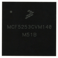
MCF5253CVM140 Freescale Semiconductor, MCF5253CVM140 Datasheet - Page 413

MCF5253CVM140
Manufacturer Part Number
MCF5253CVM140
Description
IC MPU 32BIT 140MHZ 225-MAPBGA
Manufacturer
Freescale Semiconductor
Series
MCF525xr
Datasheets
1.MCF5253VM140J.pdf
(34 pages)
2.MCF5253VM140J.pdf
(8 pages)
3.MCF5253VM140J.pdf
(648 pages)
4.MCF5253VM140J.pdf
(2 pages)
Specifications of MCF5253CVM140
Core Processor
Coldfire V2
Core Size
32-Bit
Speed
140MHz
Connectivity
CAN, EBI/EMI, I²C, QSPI, UART/USART, USB OTG
Peripherals
DMA, WDT
Program Memory Type
ROMless
Ram Size
128K x 8
Voltage - Supply (vcc/vdd)
1.08 V ~ 1.32 V
Data Converters
A/D 6x12b
Oscillator Type
External
Operating Temperature
-40°C ~ 85°C
Package / Case
225-MAPBGA
Family Name
MCF5xxx
Device Core
ColdFire V2
Device Core Size
32b
Frequency (max)
140MHz
Instruction Set Architecture
RISC
Supply Voltage 1 (typ)
1.2/3.3V
Operating Supply Voltage (max)
1.32/3.6V
Operating Supply Voltage (min)
1.08/3V
Operating Temp Range
-40C to 85C
Operating Temperature Classification
Industrial
Mounting
Surface Mount
Pin Count
225
Package Type
MA-BGA
Lead Free Status / RoHS Status
Lead free / RoHS Compliant
Number Of I /o
-
Eeprom Size
-
Program Memory Size
-
Lead Free Status / Rohs Status
Compliant
Available stocks
Company
Part Number
Manufacturer
Quantity
Price
Company:
Part Number:
MCF5253CVM140
Manufacturer:
FREESCALE
Quantity:
300
Company:
Part Number:
MCF5253CVM140
Manufacturer:
Freescale Semiconductor
Quantity:
10 000
Part Number:
MCF5253CVM140
Manufacturer:
FREESCALE
Quantity:
20 000
Company:
Part Number:
MCF5253CVM140J
Manufacturer:
Freescale Semiconductor
Quantity:
10 000
- MCF5253VM140J PDF datasheet
- MCF5253VM140J PDF datasheet #2
- MCF5253VM140J PDF datasheet #3
- MCF5253VM140J PDF datasheet #4
- Current page: 413 of 648
- Download datasheet (8Mb)
21.3.1
TCK is the dedicated JTAG test logic clock that is independent of the MCF5253 processor clock. Various
JTAG operations occur on the rising or falling edge of TCK. The internal JTAG controller logic is designed
such that holding TCK high or low for an indefinite period of time will not cause the JTAG test logic to
lose state information. If TCK is not used, it should be tied to Vdd. There is an internal pullup connected
to this pin.
21.3.2
The TEST[2:0] signals determine the function of this dual-purpose pin. If TEST[2:0]=001, the DSCLK
function is selected. If TEST[2:0]= 000, the TRST function is selected, the pin has an internal pullup and
the JTAG reset is executed. For all other modes the signal is forced internally to its active value. TEST[2:0]
should not be changed while RSTI is asserted.
When used as TRST, this pin asynchronously resets the internal JTAG controller to the test logic reset
state, causing the JTAG instruction register to choose the “idcode” command. When this occurs, all the
JTAG logic is benign and will not interfere with the normal functionality of the MCF5253 processor.
Although this signal is asynchronous, Freescale recommends that TRST make only a 0 to 1 (asserted to
negated) transition while TMS is held at a logic 1 value. TRST has an internal pullup so that if it is not
driven low its value will default to a logic level of 1. However, if TRST is not used, it can either be tied to
ground or, if TCK is clocked, it can be tied to VDD. The former connection will place the JTAG controller
in the test logic reset state immediately, while the later connection will cause the JTAG controller (if TMS
is a logic 1) to eventually end up in the test logic reset state after 5 clocks of TCK.
This pin is also used as the development serial clock (DSCLK) for the serial interface to the debug
module.The maximum frequency for the DSCLK signal is 1/2 the SYSCLK frequency.
21.3.3
The TEST[2:0] signals determine this pin’s dual function. If TEST[2:0] =001, the BKPT function is
selected. If TEST[2:0] = 000, then the TMS function is selected. TEST[2:0] should not change while RSTI
is asserted. When used as TMS, this input signal provides the JTAG controller with information to
determine which test operation mode should be performed. The value of TMS and current state of the
internal 16-state JTAG controller state machine at the rising edge of TCK determine whether the JTAG
controller holds its current state or advances to the next state. This directly controls whether JTAG data or
Freescale Semiconductor
Test Clock (TCK)
Test Reset/Development Serial Clock (TRST/DSCLK)
Test Mode Select/ Breakpoint (TMS/BKPT)
TRST
TDO
Pin
TDI
A serial test data input with a default internal pullup resistor that is sampled on the rising
edge of TCK.
A tri-state test data output that is actively driven only in the Shift-IR and Shift-DR controller
states and only updates on the falling edge of TCK.
An active-low asynchronous reset with a default internal pullup resistor that forces the TAP
controller into the test-logic-reset state.
Table 21-1. JTAG Pin Descriptions
MCF5253 Reference Manual, Rev. 1
Description
IEEE 1149.1 Test Access Port (JTAG)
21-3
Related parts for MCF5253CVM140
Image
Part Number
Description
Manufacturer
Datasheet
Request
R
Part Number:
Description:
Mcf5253 Coldfire? Microprocessor Data Sheet
Manufacturer:
Freescale Semiconductor, Inc
Datasheet:
Part Number:
Description:
Manufacturer:
Freescale Semiconductor, Inc
Datasheet:
Part Number:
Description:
Manufacturer:
Freescale Semiconductor, Inc
Datasheet:
Part Number:
Description:
Manufacturer:
Freescale Semiconductor, Inc
Datasheet:
Part Number:
Description:
Manufacturer:
Freescale Semiconductor, Inc
Datasheet:
Part Number:
Description:
Manufacturer:
Freescale Semiconductor, Inc
Datasheet:
Part Number:
Description:
Manufacturer:
Freescale Semiconductor, Inc
Datasheet:
Part Number:
Description:
Manufacturer:
Freescale Semiconductor, Inc
Datasheet:
Part Number:
Description:
Manufacturer:
Freescale Semiconductor, Inc
Datasheet:
Part Number:
Description:
Manufacturer:
Freescale Semiconductor, Inc
Datasheet:
Part Number:
Description:
Manufacturer:
Freescale Semiconductor, Inc
Datasheet:
Part Number:
Description:
Manufacturer:
Freescale Semiconductor, Inc
Datasheet:
Part Number:
Description:
Manufacturer:
Freescale Semiconductor, Inc
Datasheet:
Part Number:
Description:
Manufacturer:
Freescale Semiconductor, Inc
Datasheet:
Part Number:
Description:
Manufacturer:
Freescale Semiconductor, Inc
Datasheet:


