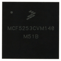
MCF5253CVM140 Freescale Semiconductor, MCF5253CVM140 Datasheet - Page 289

MCF5253CVM140
Manufacturer Part Number
MCF5253CVM140
Description
IC MPU 32BIT 140MHZ 225-MAPBGA
Manufacturer
Freescale Semiconductor
Series
MCF525xr
Datasheets
1.MCF5253VM140J.pdf
(34 pages)
2.MCF5253VM140J.pdf
(8 pages)
3.MCF5253VM140J.pdf
(648 pages)
4.MCF5253VM140J.pdf
(2 pages)
Specifications of MCF5253CVM140
Core Processor
Coldfire V2
Core Size
32-Bit
Speed
140MHz
Connectivity
CAN, EBI/EMI, I²C, QSPI, UART/USART, USB OTG
Peripherals
DMA, WDT
Program Memory Type
ROMless
Ram Size
128K x 8
Voltage - Supply (vcc/vdd)
1.08 V ~ 1.32 V
Data Converters
A/D 6x12b
Oscillator Type
External
Operating Temperature
-40°C ~ 85°C
Package / Case
225-MAPBGA
Family Name
MCF5xxx
Device Core
ColdFire V2
Device Core Size
32b
Frequency (max)
140MHz
Instruction Set Architecture
RISC
Supply Voltage 1 (typ)
1.2/3.3V
Operating Supply Voltage (max)
1.32/3.6V
Operating Supply Voltage (min)
1.08/3V
Operating Temp Range
-40C to 85C
Operating Temperature Classification
Industrial
Mounting
Surface Mount
Pin Count
225
Package Type
MA-BGA
Lead Free Status / RoHS Status
Lead free / RoHS Compliant
Number Of I /o
-
Eeprom Size
-
Program Memory Size
-
Lead Free Status / Rohs Status
Compliant
Available stocks
Company
Part Number
Manufacturer
Quantity
Price
Company:
Part Number:
MCF5253CVM140
Manufacturer:
FREESCALE
Quantity:
300
Company:
Part Number:
MCF5253CVM140
Manufacturer:
Freescale Semiconductor
Quantity:
10 000
Part Number:
MCF5253CVM140
Manufacturer:
FREESCALE
Quantity:
20 000
Company:
Part Number:
MCF5253CVM140J
Manufacturer:
Freescale Semiconductor
Quantity:
10 000
- MCF5253VM140J PDF datasheet
- MCF5253VM140J PDF datasheet #2
- MCF5253VM140J PDF datasheet #3
- MCF5253VM140J PDF datasheet #4
- Current page: 289 of 648
- Download datasheet (8Mb)
choose to delay a standard period after serial transfer is complete or can specify a delay period. Writing a
value to QDLYR[DTL] specifies a delay period. The DT bit in command RAM determines whether the
standard delay period (DT = 0) or the specified delay period (DT = 1) is used. The following expression
is used to calculate the delay:
Delay after transfer = 32 × QDLYR[DTL] /SYSCLK frequency (DT = 1)
where QDLYR[DTL] has a range of 2 to 255.
A zero value for DTL causes a delay-after-transfer value of 8192/SYSCLK frequency.
Standard delay after transfer = 17/SYSCLK frequency (DT = 0)
Adequate delay between transfers must be specified for long data streams because the QSPI module
requires time to load a transmit RAM entry for transfer. Receiving devices need at least the standard delay
between successive transfers. If SYSCLK is operating at a slower rate, the delay between transfers must
be increased proportionately.
16.3.4
There are two transfer length options. The user can choose a default value of 8 bits or a programmed value
of 8 to 16 bits inclusive. The programmed value must be written into QMR[BITS]. The bits per transfer
enable (BITSE) field in the command RAM determines whether the default value (BITSE = 0) or the
BITS[3–0] value (BITSE = 1) is used. QMR[BITS] gives the required number of bits to be transferred.
16.3.5
Operation is initiated by setting QDLYR[SPE]. Shortly after QDLYR[SPE] is set, the QSPI executes the
command at the command RAM address pointed to by QWR[NEWQP]. Data in transmit RAM is loaded
into the data shift register and transmitted. Data that is simultaneously received is stored in the receive
RAM.
When the proper number of bits has been transferred, the QSPI stores the working queue pointer value in
QWR[CPTQP], increments the working queue pointer, and loads the next data for transfer from the
transmit RAM. The command pointed to by the incremented working queue pointer is executed next
unless a new value has been written to QWR[NEWQP]. If a new queue pointer value is written while a
transfer is in progress, then that transfer is completed normally.
When the CONT bit in the command RAM is set, the QSPI_CS signals are asserted between transfers.
When CONT is cleared, QSPI_CS[3:0] are negated between transfers. The QSPI_CS signals are not high
impedance.
When the QSPI reaches the end of the queue, it asserts QIR[SPIF]. If QIR[SPIFE] is set, an interrupt
request is generated when QIR[SPIF] is asserted. Then the QSPI clears QDLYR[SPE] and stops, unless
wraparound mode is enabled.
Wraparound mode is enabled by setting QWR[WREN]. The queue can wrap to pointer address 0x0, or to
the address specified by QWR[NEWQP], depending on the state of QWR[WRTO].
Freescale Semiconductor
Transfer Length
Data Transfer
MCF5253 Reference Manual, Rev. 1
Queued Serial Peripheral Interface (QSPI) Module
16-7
Related parts for MCF5253CVM140
Image
Part Number
Description
Manufacturer
Datasheet
Request
R
Part Number:
Description:
Mcf5253 Coldfire? Microprocessor Data Sheet
Manufacturer:
Freescale Semiconductor, Inc
Datasheet:
Part Number:
Description:
Manufacturer:
Freescale Semiconductor, Inc
Datasheet:
Part Number:
Description:
Manufacturer:
Freescale Semiconductor, Inc
Datasheet:
Part Number:
Description:
Manufacturer:
Freescale Semiconductor, Inc
Datasheet:
Part Number:
Description:
Manufacturer:
Freescale Semiconductor, Inc
Datasheet:
Part Number:
Description:
Manufacturer:
Freescale Semiconductor, Inc
Datasheet:
Part Number:
Description:
Manufacturer:
Freescale Semiconductor, Inc
Datasheet:
Part Number:
Description:
Manufacturer:
Freescale Semiconductor, Inc
Datasheet:
Part Number:
Description:
Manufacturer:
Freescale Semiconductor, Inc
Datasheet:
Part Number:
Description:
Manufacturer:
Freescale Semiconductor, Inc
Datasheet:
Part Number:
Description:
Manufacturer:
Freescale Semiconductor, Inc
Datasheet:
Part Number:
Description:
Manufacturer:
Freescale Semiconductor, Inc
Datasheet:
Part Number:
Description:
Manufacturer:
Freescale Semiconductor, Inc
Datasheet:
Part Number:
Description:
Manufacturer:
Freescale Semiconductor, Inc
Datasheet:
Part Number:
Description:
Manufacturer:
Freescale Semiconductor, Inc
Datasheet:


