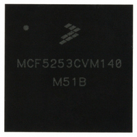
MCF5253CVM140 Freescale Semiconductor, MCF5253CVM140 Datasheet - Page 375

MCF5253CVM140
Manufacturer Part Number
MCF5253CVM140
Description
IC MPU 32BIT 140MHZ 225-MAPBGA
Manufacturer
Freescale Semiconductor
Series
MCF525xr
Datasheets
1.MCF5253VM140J.pdf
(34 pages)
2.MCF5253VM140J.pdf
(8 pages)
3.MCF5253VM140J.pdf
(648 pages)
4.MCF5253VM140J.pdf
(2 pages)
Specifications of MCF5253CVM140
Core Processor
Coldfire V2
Core Size
32-Bit
Speed
140MHz
Connectivity
CAN, EBI/EMI, I²C, QSPI, UART/USART, USB OTG
Peripherals
DMA, WDT
Program Memory Type
ROMless
Ram Size
128K x 8
Voltage - Supply (vcc/vdd)
1.08 V ~ 1.32 V
Data Converters
A/D 6x12b
Oscillator Type
External
Operating Temperature
-40°C ~ 85°C
Package / Case
225-MAPBGA
Family Name
MCF5xxx
Device Core
ColdFire V2
Device Core Size
32b
Frequency (max)
140MHz
Instruction Set Architecture
RISC
Supply Voltage 1 (typ)
1.2/3.3V
Operating Supply Voltage (max)
1.32/3.6V
Operating Supply Voltage (min)
1.08/3V
Operating Temp Range
-40C to 85C
Operating Temperature Classification
Industrial
Mounting
Surface Mount
Pin Count
225
Package Type
MA-BGA
Lead Free Status / RoHS Status
Lead free / RoHS Compliant
Number Of I /o
-
Eeprom Size
-
Program Memory Size
-
Lead Free Status / Rohs Status
Compliant
Available stocks
Company
Part Number
Manufacturer
Quantity
Price
Company:
Part Number:
MCF5253CVM140
Manufacturer:
FREESCALE
Quantity:
300
Company:
Part Number:
MCF5253CVM140
Manufacturer:
Freescale Semiconductor
Quantity:
10 000
Part Number:
MCF5253CVM140
Manufacturer:
FREESCALE
Quantity:
20 000
Company:
Part Number:
MCF5253CVM140J
Manufacturer:
Freescale Semiconductor
Quantity:
10 000
- MCF5253VM140J PDF datasheet
- MCF5253VM140J PDF datasheet #2
- MCF5253VM140J PDF datasheet #3
- MCF5253VM140J PDF datasheet #4
- Current page: 375 of 648
- Download datasheet (8Mb)
configuration. This opcode also generates the special PST encoding ($4) when executed, followed by the
appropriate marker and then the data transfer on the DDATA outputs. The length of the data transfer is
dependent on the operand size of the WDDATA instruction.
20.2.1.5
This encoding is generated whenever a taken branch is executed. For certain opcodes, the branch target
address may be optionally displayed on DDATA depending on the control parameters contained in the
configuration/status register (CSR). The number of bytes of the address to be displayed is also controlled
in the CSR and indicated by the PST marker value immediately preceding the DDATA outputs.
The bytes are always displayed in a least-significant to most-significant order. The processor captures only
those target addresses associated with taken branches using a variant addressing mode. For example, all
JMP and JSR instructions using address register indirect or indexed addressing modes, all RTE and RTS
instructions as well as all exception vectors.
The simplest example of a branch instruction using a variant address is the compiled code for a C language
“case” statement. Typically, the evaluation of this statement uses the variable of an expression as an index
into a table of offsets, where each offset points to a unique case within the structure. For these types of
change-of-flow operations, the ColdFire processor uses the debug pins to output a sequence of information
on successive processor clock cycles:
Another example of a variant branch instruction would be a JMP (A0) instruction.
outputs of the PST and DDATA signals when a JMP (A0) instruction executed, assuming the CSR is
programmed to display the lower two bytes of an address.
PST is driven with a $5 indicating a taken branch. In the second cycle, PST is driven with a marker value
of $9 indicating a two-byte address that is displayed four bits at a time on the DDATA signals over the next
four clock cycles. The remaining four clock cycles display the lower two-bytes of the address (A0), least
significant nibble to most significant nibble. The output of the PST signals after the JMP instruction
completes is dependent on the target instruction. The PST can continue with the next instruction before the
address has completely displayed on the DDATA because of the DDATA FIFO. If the FIFO is full and the
Freescale Semiconductor
1. Identify a taken branch has been executed using the PST pins ($5).
2. Using the PST pins, optionally signal the target address is to be displayed on the DDATA pins. The
3. The new target address is optionally available on subsequent cycles using the nibble-wide DDATA
PSTCLK
encoding ($9, $A, $B) identifies the number of bytes that are displayed.
port. The number of bytes of the target address displayed on this port is a configurable parameter
(2, 3, or 4 bytes).
DData
PST
Begin Execution of Taken Branch (PST = $5)
$5
$0
Figure 20-2. Example PST/DDATA Diagram
$9
$0
MCF5253 Reference Manual, Rev. 1
A[3:0]
A[7:4]
A[11:8]
Background Debug Mode (BDM) Interface
A[15:12]
Figure 20-2
shows the
20-5
Related parts for MCF5253CVM140
Image
Part Number
Description
Manufacturer
Datasheet
Request
R
Part Number:
Description:
Mcf5253 Coldfire? Microprocessor Data Sheet
Manufacturer:
Freescale Semiconductor, Inc
Datasheet:
Part Number:
Description:
Manufacturer:
Freescale Semiconductor, Inc
Datasheet:
Part Number:
Description:
Manufacturer:
Freescale Semiconductor, Inc
Datasheet:
Part Number:
Description:
Manufacturer:
Freescale Semiconductor, Inc
Datasheet:
Part Number:
Description:
Manufacturer:
Freescale Semiconductor, Inc
Datasheet:
Part Number:
Description:
Manufacturer:
Freescale Semiconductor, Inc
Datasheet:
Part Number:
Description:
Manufacturer:
Freescale Semiconductor, Inc
Datasheet:
Part Number:
Description:
Manufacturer:
Freescale Semiconductor, Inc
Datasheet:
Part Number:
Description:
Manufacturer:
Freescale Semiconductor, Inc
Datasheet:
Part Number:
Description:
Manufacturer:
Freescale Semiconductor, Inc
Datasheet:
Part Number:
Description:
Manufacturer:
Freescale Semiconductor, Inc
Datasheet:
Part Number:
Description:
Manufacturer:
Freescale Semiconductor, Inc
Datasheet:
Part Number:
Description:
Manufacturer:
Freescale Semiconductor, Inc
Datasheet:
Part Number:
Description:
Manufacturer:
Freescale Semiconductor, Inc
Datasheet:
Part Number:
Description:
Manufacturer:
Freescale Semiconductor, Inc
Datasheet:


