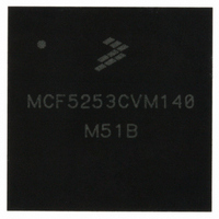
MCF5253CVM140 Freescale Semiconductor, MCF5253CVM140 Datasheet - Page 142

MCF5253CVM140
Manufacturer Part Number
MCF5253CVM140
Description
IC MPU 32BIT 140MHZ 225-MAPBGA
Manufacturer
Freescale Semiconductor
Series
MCF525xr
Datasheets
1.MCF5253VM140J.pdf
(34 pages)
2.MCF5253VM140J.pdf
(8 pages)
3.MCF5253VM140J.pdf
(648 pages)
4.MCF5253VM140J.pdf
(2 pages)
Specifications of MCF5253CVM140
Core Processor
Coldfire V2
Core Size
32-Bit
Speed
140MHz
Connectivity
CAN, EBI/EMI, I²C, QSPI, UART/USART, USB OTG
Peripherals
DMA, WDT
Program Memory Type
ROMless
Ram Size
128K x 8
Voltage - Supply (vcc/vdd)
1.08 V ~ 1.32 V
Data Converters
A/D 6x12b
Oscillator Type
External
Operating Temperature
-40°C ~ 85°C
Package / Case
225-MAPBGA
Family Name
MCF5xxx
Device Core
ColdFire V2
Device Core Size
32b
Frequency (max)
140MHz
Instruction Set Architecture
RISC
Supply Voltage 1 (typ)
1.2/3.3V
Operating Supply Voltage (max)
1.32/3.6V
Operating Supply Voltage (min)
1.08/3V
Operating Temp Range
-40C to 85C
Operating Temperature Classification
Industrial
Mounting
Surface Mount
Pin Count
225
Package Type
MA-BGA
Lead Free Status / RoHS Status
Lead free / RoHS Compliant
Number Of I /o
-
Eeprom Size
-
Program Memory Size
-
Lead Free Status / Rohs Status
Compliant
Available stocks
Company
Part Number
Manufacturer
Quantity
Price
Company:
Part Number:
MCF5253CVM140
Manufacturer:
FREESCALE
Quantity:
300
Company:
Part Number:
MCF5253CVM140
Manufacturer:
Freescale Semiconductor
Quantity:
10 000
Part Number:
MCF5253CVM140
Manufacturer:
FREESCALE
Quantity:
20 000
Company:
Part Number:
MCF5253CVM140J
Manufacturer:
Freescale Semiconductor
Quantity:
10 000
- MCF5253VM140J PDF datasheet
- MCF5253VM140J PDF datasheet #2
- MCF5253VM140J PDF datasheet #3
- MCF5253VM140J PDF datasheet #4
- Current page: 142 of 648
- Download datasheet (8Mb)
Bus Operation
The MCF5253 converts misaligned operand accesses that are noncachable to a sequence of aligned
accesses.
requiring more than one bus cycle. The slave device supplies the byte and acknowledges the data transfer.
The next two bytes are transferred during the second cycle. During the third cycle, the byte offset is now
$0; the port supplies the final byte and the operation is complete.
illustrated in
cycles.
8.7
The MCF5253 processor supports one type of reset which resets the entire MCF5253: the external master
reset input (RSTI).
To perform a master reset, an external device asserts the reset input pin (RSTI). When power is applied to
the system, external circuitry should assert RSTI for a minimum of 16 CRIN cycles after Vcc is within
tolerance.
relationships among V
must be stable by the time V
oscillating as V
random states of internal flip-flops on power up. RSTI is internally synchronized for two CRIN cycles
before being used and must meet the specified setup and hold times in relationship to CRIN to be
recognized.
8-14
Figure 8-14
Reset Operation
Figure 8-16
Figure 8-15
DD
TRANSFER 1
TRANSFER 2
TRANSFER 1
TRANSFER 2
TRANSFER 3
is ramped up to clear out contention internal to the MCF5253 processor caused by the
illustrates the transfer of a longword operand from a byte address to a 32-bit port,
DD
is a functional timing diagram of the master reset operation, illustrating
, RSTI, mode selects, and bus signals. The crystal oscillation on CRIN, CROUT
except that the operand is word-sized and the transfer requires only two bus
DD
31
31
Figure 8-14. Misaligned Longword Transfer
reaches the minimum operating specification. The crystal should start
Figure 8-15. Misaligned Word Transfer
OP 0
OP 0
–
–
–
MCF5253 Reference Manual, Rev. 1
24 23
24 23
OP 3
–
–
–
–
16 15
16 15
Figure 8-14
OP 2
–
–
–
–
8 7
8
7
is similar to the example
OP 1
OP 1
–
–
–
Freescale Semiconductor
0
0
Related parts for MCF5253CVM140
Image
Part Number
Description
Manufacturer
Datasheet
Request
R
Part Number:
Description:
Mcf5253 Coldfire? Microprocessor Data Sheet
Manufacturer:
Freescale Semiconductor, Inc
Datasheet:
Part Number:
Description:
Manufacturer:
Freescale Semiconductor, Inc
Datasheet:
Part Number:
Description:
Manufacturer:
Freescale Semiconductor, Inc
Datasheet:
Part Number:
Description:
Manufacturer:
Freescale Semiconductor, Inc
Datasheet:
Part Number:
Description:
Manufacturer:
Freescale Semiconductor, Inc
Datasheet:
Part Number:
Description:
Manufacturer:
Freescale Semiconductor, Inc
Datasheet:
Part Number:
Description:
Manufacturer:
Freescale Semiconductor, Inc
Datasheet:
Part Number:
Description:
Manufacturer:
Freescale Semiconductor, Inc
Datasheet:
Part Number:
Description:
Manufacturer:
Freescale Semiconductor, Inc
Datasheet:
Part Number:
Description:
Manufacturer:
Freescale Semiconductor, Inc
Datasheet:
Part Number:
Description:
Manufacturer:
Freescale Semiconductor, Inc
Datasheet:
Part Number:
Description:
Manufacturer:
Freescale Semiconductor, Inc
Datasheet:
Part Number:
Description:
Manufacturer:
Freescale Semiconductor, Inc
Datasheet:
Part Number:
Description:
Manufacturer:
Freescale Semiconductor, Inc
Datasheet:
Part Number:
Description:
Manufacturer:
Freescale Semiconductor, Inc
Datasheet:


