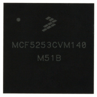
MCF5253CVM140 Freescale Semiconductor, MCF5253CVM140 Datasheet - Page 180

MCF5253CVM140
Manufacturer Part Number
MCF5253CVM140
Description
IC MPU 32BIT 140MHZ 225-MAPBGA
Manufacturer
Freescale Semiconductor
Series
MCF525xr
Datasheets
1.MCF5253VM140J.pdf
(34 pages)
2.MCF5253VM140J.pdf
(8 pages)
3.MCF5253VM140J.pdf
(648 pages)
4.MCF5253VM140J.pdf
(2 pages)
Specifications of MCF5253CVM140
Core Processor
Coldfire V2
Core Size
32-Bit
Speed
140MHz
Connectivity
CAN, EBI/EMI, I²C, QSPI, UART/USART, USB OTG
Peripherals
DMA, WDT
Program Memory Type
ROMless
Ram Size
128K x 8
Voltage - Supply (vcc/vdd)
1.08 V ~ 1.32 V
Data Converters
A/D 6x12b
Oscillator Type
External
Operating Temperature
-40°C ~ 85°C
Package / Case
225-MAPBGA
Family Name
MCF5xxx
Device Core
ColdFire V2
Device Core Size
32b
Frequency (max)
140MHz
Instruction Set Architecture
RISC
Supply Voltage 1 (typ)
1.2/3.3V
Operating Supply Voltage (max)
1.32/3.6V
Operating Supply Voltage (min)
1.08/3V
Operating Temp Range
-40C to 85C
Operating Temperature Classification
Industrial
Mounting
Surface Mount
Pin Count
225
Package Type
MA-BGA
Lead Free Status / RoHS Status
Lead free / RoHS Compliant
Number Of I /o
-
Eeprom Size
-
Program Memory Size
-
Lead Free Status / Rohs Status
Compliant
Available stocks
Company
Part Number
Manufacturer
Quantity
Price
Company:
Part Number:
MCF5253CVM140
Manufacturer:
FREESCALE
Quantity:
300
Company:
Part Number:
MCF5253CVM140
Manufacturer:
Freescale Semiconductor
Quantity:
10 000
Part Number:
MCF5253CVM140
Manufacturer:
FREESCALE
Quantity:
20 000
Company:
Part Number:
MCF5253CVM140J
Manufacturer:
Freescale Semiconductor
Quantity:
10 000
- MCF5253VM140J PDF datasheet
- MCF5253VM140J PDF datasheet #2
- MCF5253VM140J PDF datasheet #3
- MCF5253VM140J PDF datasheet #4
- Current page: 180 of 648
- Download datasheet (8Mb)
Chip Select Module
10.3.3
CS0 is the global (boot) chip select and it allows address decoding for the boot ROM before system
initialization occurs. Its operation differs from the other external chip-select outputs following a system
reset. Its operation is also dependent on the pull-up or pull-down status of address line A23 at power-on
reset, see
After system reset, CS0 is asserted for every external access. Internal accesses can be made to go external
by setting the internal bus arbitration control (IARBCTRL) bit of the default bus master (MPARK) register
in the system integration module (SIM). No other chip-select can be used while CS0 is a global chip select.
CS0 operates in this manner until the valid bit is set in chip select mask register CSMR0[0], at which point
CS1 may be used. At reset, the port size and automatic acknowledge functions of the global chip-select are
determined.
The reset state of CS0 is always auto-acknowledge (AA) with 15 wait states and the port size is 16-bits.
Provided the required address range is first loaded into chip select address register (CSAR), CS0 can be
programmed to continue to decode for a range of addresses after the valid (V) bit is set. After the V-bit is
set for CS0, global chip-select can be restored only with another system reset.
10.4
The Chip Select module registers and their field descriptions are provided in this section followed by a
code example to initialize the chip selects.
10.4.1
Table 10-2
zeros.
The CSCRs should be accessed through a MOV.L to longword address offset they belong to, while reading
and writing to the lower 16-bits of the longword data transfer (DATA[15:0]).
10-4
MBAR + 0x80
MBAR + 0x84
Address
Section 10.2.1, “CS0/CS4,”
Chip Select Memory Map and Register Definitions
1
shows the memory map of all the chip-select registers. Reading reserved locations returns
Global Chip-Select Operation
Chip Select Register Memory Map
CS0/CS4 are multiplexed, when CS0 is enabled for on-chip boot ROM
access, CS0 is used for these access and CS4 is automatically enabled as the
output for the CS0/CS4 pin.
All of these accesses are longword in length, instead of word length, even
though both the CSARs and CSCRs use only 16 bits in the 32-bits registers.
CSMR0
CSAR0
Name
Width
16
32
Table 10-2. Memory Map of Chip-Select Registers
Chip-Select Address Register–Bank 0
Chip-Select Mask Register–Bank 0
MCF5253 Reference Manual, Rev. 1
for details.
Description
NOTE
NOTE
(except V = 0)
Uninitialized
Uninitialized
Reset
2
Freescale Semiconductor
Access
R/W
R/W
Related parts for MCF5253CVM140
Image
Part Number
Description
Manufacturer
Datasheet
Request
R
Part Number:
Description:
Mcf5253 Coldfire? Microprocessor Data Sheet
Manufacturer:
Freescale Semiconductor, Inc
Datasheet:
Part Number:
Description:
Manufacturer:
Freescale Semiconductor, Inc
Datasheet:
Part Number:
Description:
Manufacturer:
Freescale Semiconductor, Inc
Datasheet:
Part Number:
Description:
Manufacturer:
Freescale Semiconductor, Inc
Datasheet:
Part Number:
Description:
Manufacturer:
Freescale Semiconductor, Inc
Datasheet:
Part Number:
Description:
Manufacturer:
Freescale Semiconductor, Inc
Datasheet:
Part Number:
Description:
Manufacturer:
Freescale Semiconductor, Inc
Datasheet:
Part Number:
Description:
Manufacturer:
Freescale Semiconductor, Inc
Datasheet:
Part Number:
Description:
Manufacturer:
Freescale Semiconductor, Inc
Datasheet:
Part Number:
Description:
Manufacturer:
Freescale Semiconductor, Inc
Datasheet:
Part Number:
Description:
Manufacturer:
Freescale Semiconductor, Inc
Datasheet:
Part Number:
Description:
Manufacturer:
Freescale Semiconductor, Inc
Datasheet:
Part Number:
Description:
Manufacturer:
Freescale Semiconductor, Inc
Datasheet:
Part Number:
Description:
Manufacturer:
Freescale Semiconductor, Inc
Datasheet:
Part Number:
Description:
Manufacturer:
Freescale Semiconductor, Inc
Datasheet:


