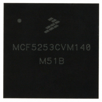
MCF5253CVM140 Freescale Semiconductor, MCF5253CVM140 Datasheet - Page 136

MCF5253CVM140
Manufacturer Part Number
MCF5253CVM140
Description
IC MPU 32BIT 140MHZ 225-MAPBGA
Manufacturer
Freescale Semiconductor
Series
MCF525xr
Datasheets
1.MCF5253VM140J.pdf
(34 pages)
2.MCF5253VM140J.pdf
(8 pages)
3.MCF5253VM140J.pdf
(648 pages)
4.MCF5253VM140J.pdf
(2 pages)
Specifications of MCF5253CVM140
Core Processor
Coldfire V2
Core Size
32-Bit
Speed
140MHz
Connectivity
CAN, EBI/EMI, I²C, QSPI, UART/USART, USB OTG
Peripherals
DMA, WDT
Program Memory Type
ROMless
Ram Size
128K x 8
Voltage - Supply (vcc/vdd)
1.08 V ~ 1.32 V
Data Converters
A/D 6x12b
Oscillator Type
External
Operating Temperature
-40°C ~ 85°C
Package / Case
225-MAPBGA
Family Name
MCF5xxx
Device Core
ColdFire V2
Device Core Size
32b
Frequency (max)
140MHz
Instruction Set Architecture
RISC
Supply Voltage 1 (typ)
1.2/3.3V
Operating Supply Voltage (max)
1.32/3.6V
Operating Supply Voltage (min)
1.08/3V
Operating Temp Range
-40C to 85C
Operating Temperature Classification
Industrial
Mounting
Surface Mount
Pin Count
225
Package Type
MA-BGA
Lead Free Status / RoHS Status
Lead free / RoHS Compliant
Number Of I /o
-
Eeprom Size
-
Program Memory Size
-
Lead Free Status / Rohs Status
Compliant
Available stocks
Company
Part Number
Manufacturer
Quantity
Price
Company:
Part Number:
MCF5253CVM140
Manufacturer:
FREESCALE
Quantity:
300
Company:
Part Number:
MCF5253CVM140
Manufacturer:
Freescale Semiconductor
Quantity:
10 000
Part Number:
MCF5253CVM140
Manufacturer:
FREESCALE
Quantity:
20 000
Company:
Part Number:
MCF5253CVM140J
Manufacturer:
Freescale Semiconductor
Quantity:
10 000
- MCF5253VM140J PDF datasheet
- MCF5253VM140J PDF datasheet #2
- MCF5253VM140J PDF datasheet #3
- MCF5253VM140J PDF datasheet #4
- Current page: 136 of 648
- Download datasheet (8Mb)
1
2
Bus Operation
8.5.3
The Write cycle as shown in
Register (CSR) is programmed to value “0000”. The CS low time is increased with n clocks if n is
programmed into the WS field.
During a write cycle, the MCF5253 sends data to the memory or to a peripheral device.
The write cycle flowchart is
8-8
STATE 3
STATE 4
STATE 5
The external device has a maximum of 1.5 BCLK cycles after the start of S4 to three-state the data bus after data is sampled
in S3 during a read cycle. This applies to basic read cycles and the last transfer of a burst.
The MCF5253 would not drive out data for a minimum of two BCLK cycles. However, another slave device may start driving
the bus as soon as its chip select is asserted. Chip select may be asserted at the beginning of S1, so bus drive must stop
before the end of S0. Under these conditions, data contention on the bus would not exist.
Name
State
1. Sample TA Low
2. Tri-State Data on D[31:16]
3. Start Next Cycle
1. Set RW to Write
2. Place Address on A[23:1]
3. Drive Data on D[31:16]
Data is made available by the external device and is sampled on the rising edge of BCLK with TA asserted. If TA
not asserted before the rising edge of BCLK at the end of the first clock cycle, the MCF5253 inserts wait states
(full clock cycles) until TA is asserted. If internal TA is requested (auto-acknowledge enabled in the chip select
control register, CSCR) then TA is generated internally by the chip select module.
During state 4, TA should be negated by the external device or if auto-acknowledge is enabled will be negated
internally by the chip select module.
CS and OE are negated on the falling edge of state 5 (S5). The MCF5253 stops driving the address lines and RW
on the rising edge of BCLK, terminating the read cycle. The external device must have its drive from the bus. The
external device must stop driving the bus.
The rising edge of BCLK may be the start of state 0 for the next access cycle.
Write Cycle
MCF5253
Figure
Figure 8-6.
Table 8-6. Read Cycle States (continued)
8-6., will occur if the wait cycle field (WS) in the Chip Select Control
Figure 8-5. Write Cycle Flowchart
MCF5253 Reference Manual, Rev. 1
Write cycle timing diagram is
Description
1. Decode Address
2. Store Data on D[31:16]
3. CS unit asserts TA (internal termination) or assert TA
externally for 1 BCLK cycle
(external termination).
1,2
External Memory/Device
Figure
8-7.
Freescale Semiconductor
Related parts for MCF5253CVM140
Image
Part Number
Description
Manufacturer
Datasheet
Request
R
Part Number:
Description:
Mcf5253 Coldfire? Microprocessor Data Sheet
Manufacturer:
Freescale Semiconductor, Inc
Datasheet:
Part Number:
Description:
Manufacturer:
Freescale Semiconductor, Inc
Datasheet:
Part Number:
Description:
Manufacturer:
Freescale Semiconductor, Inc
Datasheet:
Part Number:
Description:
Manufacturer:
Freescale Semiconductor, Inc
Datasheet:
Part Number:
Description:
Manufacturer:
Freescale Semiconductor, Inc
Datasheet:
Part Number:
Description:
Manufacturer:
Freescale Semiconductor, Inc
Datasheet:
Part Number:
Description:
Manufacturer:
Freescale Semiconductor, Inc
Datasheet:
Part Number:
Description:
Manufacturer:
Freescale Semiconductor, Inc
Datasheet:
Part Number:
Description:
Manufacturer:
Freescale Semiconductor, Inc
Datasheet:
Part Number:
Description:
Manufacturer:
Freescale Semiconductor, Inc
Datasheet:
Part Number:
Description:
Manufacturer:
Freescale Semiconductor, Inc
Datasheet:
Part Number:
Description:
Manufacturer:
Freescale Semiconductor, Inc
Datasheet:
Part Number:
Description:
Manufacturer:
Freescale Semiconductor, Inc
Datasheet:
Part Number:
Description:
Manufacturer:
Freescale Semiconductor, Inc
Datasheet:
Part Number:
Description:
Manufacturer:
Freescale Semiconductor, Inc
Datasheet:


