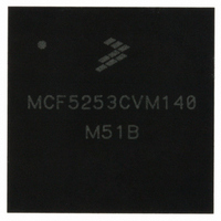
MCF5253CVM140 Freescale Semiconductor, MCF5253CVM140 Datasheet - Page 43

MCF5253CVM140
Manufacturer Part Number
MCF5253CVM140
Description
IC MPU 32BIT 140MHZ 225-MAPBGA
Manufacturer
Freescale Semiconductor
Series
MCF525xr
Datasheets
1.MCF5253VM140J.pdf
(34 pages)
2.MCF5253VM140J.pdf
(8 pages)
3.MCF5253VM140J.pdf
(648 pages)
4.MCF5253VM140J.pdf
(2 pages)
Specifications of MCF5253CVM140
Core Processor
Coldfire V2
Core Size
32-Bit
Speed
140MHz
Connectivity
CAN, EBI/EMI, I²C, QSPI, UART/USART, USB OTG
Peripherals
DMA, WDT
Program Memory Type
ROMless
Ram Size
128K x 8
Voltage - Supply (vcc/vdd)
1.08 V ~ 1.32 V
Data Converters
A/D 6x12b
Oscillator Type
External
Operating Temperature
-40°C ~ 85°C
Package / Case
225-MAPBGA
Family Name
MCF5xxx
Device Core
ColdFire V2
Device Core Size
32b
Frequency (max)
140MHz
Instruction Set Architecture
RISC
Supply Voltage 1 (typ)
1.2/3.3V
Operating Supply Voltage (max)
1.32/3.6V
Operating Supply Voltage (min)
1.08/3V
Operating Temp Range
-40C to 85C
Operating Temperature Classification
Industrial
Mounting
Surface Mount
Pin Count
225
Package Type
MA-BGA
Lead Free Status / RoHS Status
Lead free / RoHS Compliant
Number Of I /o
-
Eeprom Size
-
Program Memory Size
-
Lead Free Status / Rohs Status
Compliant
Available stocks
Company
Part Number
Manufacturer
Quantity
Price
Company:
Part Number:
MCF5253CVM140
Manufacturer:
FREESCALE
Quantity:
300
Company:
Part Number:
MCF5253CVM140
Manufacturer:
Freescale Semiconductor
Quantity:
10 000
Part Number:
MCF5253CVM140
Manufacturer:
FREESCALE
Quantity:
20 000
Company:
Part Number:
MCF5253CVM140J
Manufacturer:
Freescale Semiconductor
Quantity:
10 000
- MCF5253VM140J PDF datasheet
- MCF5253VM140J PDF datasheet #2
- MCF5253VM140J PDF datasheet #3
- MCF5253VM140J PDF datasheet #4
- Current page: 43 of 648
- Download datasheet (8Mb)
17.5 Mbits/second are possible at a CPU clock of 140 MHz. The QSPI supports master mode operation
only.
1.5.19
The MCF5253 incorporates two independent, general-purpose 16-bit timers. The output of an 8-bit
prescaler clocks each 16-bit timer. The prescaler input can be the system clock or the system clock divided
by 16. Timer0 output pin is multiplexed with SDATAO1/TOUT0/GPIO18. Upon reset, this pin is
programmed as SDATAO1. To use the TOUT0 pin function it is necessary to program the Pin
Configuration register appropriately.
1.5.20
The MCF5253 system bus allows connection of an IDE hard disk drive with a minimum of external
hardware. The external hardware consists of bus buffers for address and data and are intended to reduce
the load on the bus and prevent SDRAM and Flash accesses from propagating to the IDE bus. The control
signals for the buffers are generated in the MCF5253.
1.5.21
The six channel ADC is based on the Sigma-Delta concept with 12-bit resolution. Both the analog
comparator and digital sections are integrated in the MCF5253. An external integrator circuit
(resistor/capacitor) is required which is driven by the ADC output. A interrupt is provided when the ADC
measurement cycle is complete.
1.5.22
The interface is Sony
is no hardware support for Sony MagicGate
1.5.23
The two-wire I
serial bus that exchanges data between devices. The I
devices in the end system and is best suited for applications that need occasional bursts of rapid
communication over short distances among several devices. Bus capacitance and the number of unique
addresses limit the maximum communication length and the number of devices that can be connected.
1.5.24
There are three programmable chip selects on the MCF5253:
Freescale Semiconductor
•
Three programmable chip-select outputs (CS0/CS4, CS1 and CS2) provide signals that enable
glueless connection to external memory and peripheral circuits. The base address, access
permissions, and automatic wait-state insertion are programmable with configuration registers.
These signals also interface to 16-bit ports.
Timer Module
IDE Interface
Analog/Digital Converter (ADC)
Flash Memory Card Interface
I
Chip-Selects
2
C Module
2
C bus interface, which is compliant with the Philips I
®
Memory Stick
MCF5253 Reference Manual, Rev. 1
®
, SecureDigital and Multi-Media card compatible. However, there
™
.
2
C bus minimizes the interconnection between
2
C bus standard, is a bidirectional
MCF5253 Introduction
1-11
Related parts for MCF5253CVM140
Image
Part Number
Description
Manufacturer
Datasheet
Request
R
Part Number:
Description:
Mcf5253 Coldfire? Microprocessor Data Sheet
Manufacturer:
Freescale Semiconductor, Inc
Datasheet:
Part Number:
Description:
Manufacturer:
Freescale Semiconductor, Inc
Datasheet:
Part Number:
Description:
Manufacturer:
Freescale Semiconductor, Inc
Datasheet:
Part Number:
Description:
Manufacturer:
Freescale Semiconductor, Inc
Datasheet:
Part Number:
Description:
Manufacturer:
Freescale Semiconductor, Inc
Datasheet:
Part Number:
Description:
Manufacturer:
Freescale Semiconductor, Inc
Datasheet:
Part Number:
Description:
Manufacturer:
Freescale Semiconductor, Inc
Datasheet:
Part Number:
Description:
Manufacturer:
Freescale Semiconductor, Inc
Datasheet:
Part Number:
Description:
Manufacturer:
Freescale Semiconductor, Inc
Datasheet:
Part Number:
Description:
Manufacturer:
Freescale Semiconductor, Inc
Datasheet:
Part Number:
Description:
Manufacturer:
Freescale Semiconductor, Inc
Datasheet:
Part Number:
Description:
Manufacturer:
Freescale Semiconductor, Inc
Datasheet:
Part Number:
Description:
Manufacturer:
Freescale Semiconductor, Inc
Datasheet:
Part Number:
Description:
Manufacturer:
Freescale Semiconductor, Inc
Datasheet:
Part Number:
Description:
Manufacturer:
Freescale Semiconductor, Inc
Datasheet:


