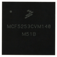
MCF5253CVM140 Freescale Semiconductor, MCF5253CVM140 Datasheet - Page 509

MCF5253CVM140
Manufacturer Part Number
MCF5253CVM140
Description
IC MPU 32BIT 140MHZ 225-MAPBGA
Manufacturer
Freescale Semiconductor
Series
MCF525xr
Datasheets
1.MCF5253VM140J.pdf
(34 pages)
2.MCF5253VM140J.pdf
(8 pages)
3.MCF5253VM140J.pdf
(648 pages)
4.MCF5253VM140J.pdf
(2 pages)
Specifications of MCF5253CVM140
Core Processor
Coldfire V2
Core Size
32-Bit
Speed
140MHz
Connectivity
CAN, EBI/EMI, I²C, QSPI, UART/USART, USB OTG
Peripherals
DMA, WDT
Program Memory Type
ROMless
Ram Size
128K x 8
Voltage - Supply (vcc/vdd)
1.08 V ~ 1.32 V
Data Converters
A/D 6x12b
Oscillator Type
External
Operating Temperature
-40°C ~ 85°C
Package / Case
225-MAPBGA
Family Name
MCF5xxx
Device Core
ColdFire V2
Device Core Size
32b
Frequency (max)
140MHz
Instruction Set Architecture
RISC
Supply Voltage 1 (typ)
1.2/3.3V
Operating Supply Voltage (max)
1.32/3.6V
Operating Supply Voltage (min)
1.08/3V
Operating Temp Range
-40C to 85C
Operating Temperature Classification
Industrial
Mounting
Surface Mount
Pin Count
225
Package Type
MA-BGA
Lead Free Status / RoHS Status
Lead free / RoHS Compliant
Number Of I /o
-
Eeprom Size
-
Program Memory Size
-
Lead Free Status / Rohs Status
Compliant
Available stocks
Company
Part Number
Manufacturer
Quantity
Price
Company:
Part Number:
MCF5253CVM140
Manufacturer:
FREESCALE
Quantity:
300
Company:
Part Number:
MCF5253CVM140
Manufacturer:
Freescale Semiconductor
Quantity:
10 000
Part Number:
MCF5253CVM140
Manufacturer:
FREESCALE
Quantity:
20 000
Company:
Part Number:
MCF5253CVM140J
Manufacturer:
Freescale Semiconductor
Quantity:
10 000
- MCF5253VM140J PDF datasheet
- MCF5253VM140J PDF datasheet #2
- MCF5253VM140J PDF datasheet #3
- MCF5253VM140J PDF datasheet #4
- Current page: 509 of 648
- Download datasheet (8Mb)
Note that the software must ensure that no interface data structure reachable by the EHCI host controller
spans a 4K-page boundary.
The data structures defined in this section are (from the host controller’s perspective) a mix of read-only
and read/writable fields. The host controller must preserve the read-only fields on all data structure writes.
24.8.1
Figure 24-35
(isochronous and interrupt). The periodic schedule is referenced from the operational registers space using
the PERIODICLISTBASE address register and the FRINDEX register. The periodic schedule is based on
an array of pointers called the Periodic Frame List. The PERIODICLISTBASE address register is
combined with the FRINDEX register to produce a memory pointer into the frame list. The Periodic Frame
List implements a sliding window of work over time.
Split transaction Interrupt, Bulk and Control are also managed using queue heads and queue element
transfer descriptors.
The periodic frame list is a 4K-page aligned array of Frame List Link pointers. The length of the frame list
may be programmable. The programmability of the periodic frame list is exported to the system software
via the HCCPARAMS register. If non-programmable, the length is 1024 elements. If programmable, the
length can be selected by the system software as one of 256, 512, or 1024 elements. An implementation
must support all three sizes. Programming the size (that is, the number of elements) is accomplished by
the system software writing the appropriate value into Frame List Size field in the USBCMD register.
Frame List Link pointers direct the host controller to the first work item in the frame’s periodic schedule
for the current micro-frame. The link pointers are aligned on DWord boundaries within the Frame List.
Figure 24-36
Freescale Semiconductor
Periodic Frame
PeriodicListBase
List Element
Operational
Registers
FRINDEX
Address
Periodic Frame List
shows the organization of the periodic schedule. This schedule is for all periodic transfers
shows the format for the Frame List Link Pointer.
1024, 512, or 256
Elements
Figure 24-35. Periodic Schedule Organization
MCF5253 Reference Manual, Rev. 1
Periodic Frame List
•
•
•
Poll Rate: N –– > 1
•
•
•
A
A
A
A
A
A
Isochronous Transfer
Descriptor(s)
8
Interrupt Queue
A
4
Heads
• • •
Universal Serial Bus Interface
1
Last
Periodic has
End of
List Mark
24-47
Related parts for MCF5253CVM140
Image
Part Number
Description
Manufacturer
Datasheet
Request
R
Part Number:
Description:
Mcf5253 Coldfire? Microprocessor Data Sheet
Manufacturer:
Freescale Semiconductor, Inc
Datasheet:
Part Number:
Description:
Manufacturer:
Freescale Semiconductor, Inc
Datasheet:
Part Number:
Description:
Manufacturer:
Freescale Semiconductor, Inc
Datasheet:
Part Number:
Description:
Manufacturer:
Freescale Semiconductor, Inc
Datasheet:
Part Number:
Description:
Manufacturer:
Freescale Semiconductor, Inc
Datasheet:
Part Number:
Description:
Manufacturer:
Freescale Semiconductor, Inc
Datasheet:
Part Number:
Description:
Manufacturer:
Freescale Semiconductor, Inc
Datasheet:
Part Number:
Description:
Manufacturer:
Freescale Semiconductor, Inc
Datasheet:
Part Number:
Description:
Manufacturer:
Freescale Semiconductor, Inc
Datasheet:
Part Number:
Description:
Manufacturer:
Freescale Semiconductor, Inc
Datasheet:
Part Number:
Description:
Manufacturer:
Freescale Semiconductor, Inc
Datasheet:
Part Number:
Description:
Manufacturer:
Freescale Semiconductor, Inc
Datasheet:
Part Number:
Description:
Manufacturer:
Freescale Semiconductor, Inc
Datasheet:
Part Number:
Description:
Manufacturer:
Freescale Semiconductor, Inc
Datasheet:
Part Number:
Description:
Manufacturer:
Freescale Semiconductor, Inc
Datasheet:


