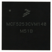
MCF5253CVM140 Freescale Semiconductor, MCF5253CVM140 Datasheet - Page 149

MCF5253CVM140
Manufacturer Part Number
MCF5253CVM140
Description
IC MPU 32BIT 140MHZ 225-MAPBGA
Manufacturer
Freescale Semiconductor
Series
MCF525xr
Datasheets
1.MCF5253VM140J.pdf
(34 pages)
2.MCF5253VM140J.pdf
(8 pages)
3.MCF5253VM140J.pdf
(648 pages)
4.MCF5253VM140J.pdf
(2 pages)
Specifications of MCF5253CVM140
Core Processor
Coldfire V2
Core Size
32-Bit
Speed
140MHz
Connectivity
CAN, EBI/EMI, I²C, QSPI, UART/USART, USB OTG
Peripherals
DMA, WDT
Program Memory Type
ROMless
Ram Size
128K x 8
Voltage - Supply (vcc/vdd)
1.08 V ~ 1.32 V
Data Converters
A/D 6x12b
Oscillator Type
External
Operating Temperature
-40°C ~ 85°C
Package / Case
225-MAPBGA
Family Name
MCF5xxx
Device Core
ColdFire V2
Device Core Size
32b
Frequency (max)
140MHz
Instruction Set Architecture
RISC
Supply Voltage 1 (typ)
1.2/3.3V
Operating Supply Voltage (max)
1.32/3.6V
Operating Supply Voltage (min)
1.08/3V
Operating Temp Range
-40C to 85C
Operating Temperature Classification
Industrial
Mounting
Surface Mount
Pin Count
225
Package Type
MA-BGA
Lead Free Status / RoHS Status
Lead free / RoHS Compliant
Number Of I /o
-
Eeprom Size
-
Program Memory Size
-
Lead Free Status / Rohs Status
Compliant
Available stocks
Company
Part Number
Manufacturer
Quantity
Price
Company:
Part Number:
MCF5253CVM140
Manufacturer:
FREESCALE
Quantity:
300
Company:
Part Number:
MCF5253CVM140
Manufacturer:
Freescale Semiconductor
Quantity:
10 000
Part Number:
MCF5253CVM140
Manufacturer:
FREESCALE
Quantity:
20 000
Company:
Part Number:
MCF5253CVM140J
Manufacturer:
Freescale Semiconductor
Quantity:
10 000
- MCF5253VM140J PDF datasheet
- MCF5253VM140J PDF datasheet #2
- MCF5253VM140J PDF datasheet #3
- MCF5253VM140J PDF datasheet #4
- Current page: 149 of 648
- Download datasheet (8Mb)
The following example shows how to set the MBAR to location $10000000 using the D0 register. A “1”
in the least significant bit validates the MBAR location. This example assumes that all accesses are valid:
Freescale Semiconductor
Address CPU + $C0E
31–30
Field
Field
29–8
Reset
Reset
UC
UD
SC
SD
BA
V
4
3
2
1
0
W
W
move.1 #$10000001,DO
movec DO,MBAR
R
R
BA31 BA30
Mask Supervisor Code space in MBAR address range.
0 Supervisor code access allowed
1 Supervisor code access masked
Mask Supervisor Data space in MBAR address range.
0 Supervisor data access allowed
1 Supervisor data access masked
Mask User Code space in MBAR address range.
0 User code access allowed
1 User code access masked
Mask User Data space in MBAR address range.
0 User data space access allowed
1 User data space access masked
This bit defines when the base address is valid:
0 MBAR address space not visible by CPU
1 MBAR address space visible by CPU
The Base Address field defines the base address for a 1024 Mbyte address range. If V-bit in MBAR2 is set, address
range Base Address to BaseAddress + $3FFF FFFF are mapped to MBAR2 space, and cannot be used for MBAR,
SDRAM or Chip Select.
Reserved, should be cleared.
31
15
0
–
Table 9-3. Module Base Address Register (MBAR) Field Descriptions (continued)
Table 9-4. Second Module Base Address Register (MBAR2)Field Descriptions
30
14
0
–
29
13
Figure 9-2. Second Module Base Address Register (MBAR2)
–
–
28
12
–
–
27
11
–
–
MCF5253 Reference Manual, Rev. 1
26
10
–
–
25
–
–
9
Description
Description
24
–
8
–
LS7
23
–
0
7
LS6
22
–
0
6
LS5
21
–
0
5
LS4
20
–
4
0
System Integration Module (SIM)
LS3
19
–
0
3
Access: User read/write
LS2
18
–
0
2
LS1
17
–
0
1
16
V
–
0
0
9-5
Related parts for MCF5253CVM140
Image
Part Number
Description
Manufacturer
Datasheet
Request
R
Part Number:
Description:
Mcf5253 Coldfire? Microprocessor Data Sheet
Manufacturer:
Freescale Semiconductor, Inc
Datasheet:
Part Number:
Description:
Manufacturer:
Freescale Semiconductor, Inc
Datasheet:
Part Number:
Description:
Manufacturer:
Freescale Semiconductor, Inc
Datasheet:
Part Number:
Description:
Manufacturer:
Freescale Semiconductor, Inc
Datasheet:
Part Number:
Description:
Manufacturer:
Freescale Semiconductor, Inc
Datasheet:
Part Number:
Description:
Manufacturer:
Freescale Semiconductor, Inc
Datasheet:
Part Number:
Description:
Manufacturer:
Freescale Semiconductor, Inc
Datasheet:
Part Number:
Description:
Manufacturer:
Freescale Semiconductor, Inc
Datasheet:
Part Number:
Description:
Manufacturer:
Freescale Semiconductor, Inc
Datasheet:
Part Number:
Description:
Manufacturer:
Freescale Semiconductor, Inc
Datasheet:
Part Number:
Description:
Manufacturer:
Freescale Semiconductor, Inc
Datasheet:
Part Number:
Description:
Manufacturer:
Freescale Semiconductor, Inc
Datasheet:
Part Number:
Description:
Manufacturer:
Freescale Semiconductor, Inc
Datasheet:
Part Number:
Description:
Manufacturer:
Freescale Semiconductor, Inc
Datasheet:
Part Number:
Description:
Manufacturer:
Freescale Semiconductor, Inc
Datasheet:


