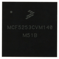
MCF5253CVM140 Freescale Semiconductor, MCF5253CVM140 Datasheet - Page 47

MCF5253CVM140
Manufacturer Part Number
MCF5253CVM140
Description
IC MPU 32BIT 140MHZ 225-MAPBGA
Manufacturer
Freescale Semiconductor
Series
MCF525xr
Datasheets
1.MCF5253VM140J.pdf
(34 pages)
2.MCF5253VM140J.pdf
(8 pages)
3.MCF5253VM140J.pdf
(648 pages)
4.MCF5253VM140J.pdf
(2 pages)
Specifications of MCF5253CVM140
Core Processor
Coldfire V2
Core Size
32-Bit
Speed
140MHz
Connectivity
CAN, EBI/EMI, I²C, QSPI, UART/USART, USB OTG
Peripherals
DMA, WDT
Program Memory Type
ROMless
Ram Size
128K x 8
Voltage - Supply (vcc/vdd)
1.08 V ~ 1.32 V
Data Converters
A/D 6x12b
Oscillator Type
External
Operating Temperature
-40°C ~ 85°C
Package / Case
225-MAPBGA
Family Name
MCF5xxx
Device Core
ColdFire V2
Device Core Size
32b
Frequency (max)
140MHz
Instruction Set Architecture
RISC
Supply Voltage 1 (typ)
1.2/3.3V
Operating Supply Voltage (max)
1.32/3.6V
Operating Supply Voltage (min)
1.08/3V
Operating Temp Range
-40C to 85C
Operating Temperature Classification
Industrial
Mounting
Surface Mount
Pin Count
225
Package Type
MA-BGA
Lead Free Status / RoHS Status
Lead free / RoHS Compliant
Number Of I /o
-
Eeprom Size
-
Program Memory Size
-
Lead Free Status / Rohs Status
Compliant
Available stocks
Company
Part Number
Manufacturer
Quantity
Price
Company:
Part Number:
MCF5253CVM140
Manufacturer:
FREESCALE
Quantity:
300
Company:
Part Number:
MCF5253CVM140
Manufacturer:
Freescale Semiconductor
Quantity:
10 000
Part Number:
MCF5253CVM140
Manufacturer:
FREESCALE
Quantity:
20 000
Company:
Part Number:
MCF5253CVM140J
Manufacturer:
Freescale Semiconductor
Quantity:
10 000
- MCF5253VM140J PDF datasheet
- MCF5253VM140J PDF datasheet #2
- MCF5253VM140J PDF datasheet #3
- MCF5253VM140J PDF datasheet #4
- Current page: 47 of 648
- Download datasheet (8Mb)
Chapter 2
Signal Description
2.1
This chapter describes the MCF5253 input and output signals. The signal descriptions as shown in
Table 2-1
ISA bus read strobe
Freescale Semiconductor
Address
Read-write control
Output enable
Data
Synchronous row
address strobe
Synchronous column
address strobe
SDRAM write enable
SDRAM upper byte
enable
SDRAM lower byte
enable
SDRAM chip selects
SDRAM clock enable
System clock
ISA bus write strobe
ISA bus wait signal
Signal Name
Overview
are grouped according to relevant functionality.
IDE_DIOR/GPIO31
A[24:1]
A[23]/GPO54
RW
OE
D[31:16]
SDRAS/GPIO59
SDCAS/GPIO39
SDWE/GPIO38
SDUDQM/GPO53
SDLDQM/GPO52
SD_CS0/GPIO60
BCLKE/GPIO63
BCLK/GPIO40
(CS2)
IDE_DIOW/GPIO32
(CS2)
IDE_IORDY/GPIO33
Mnemonic
Table 2-1. MCF5253 Signal Index
MCF5253 Reference Manual, Rev. 1
24 address lines—address 23 is
multiplexed with GPO54 and address
24 is multiplexed with A20 (SDRAM
access only).
Bus write enable—indicates if read or
write cycle in progress.
Output enable for asynchronous
memories connected to chip selects
Data bus used to transfer word data
Row address strobe for external
SDRAM
Column address strobe for external
SDRAM
Write enable for external SDRAM
Upper byte enable—indicates during
write cycle if high byte is written.
Lower byte enable—indicates during
write cycle if low byte is written.
SDRAM chip select
SDRAM clock enable
SDRAM clock output
1 ISA bus read strobe and 1 ISA bus
write strobe—allow connection of an
independent ISA bus peripheral, such
as an IDE slave device.
ISA bus wait line available for both
busses
Function
Output
Input/
In/Out
In/Out
In/Out
In/Out
In/Out
In/Out
Out
Out
Out
Out
Out
Out
Out
Out
Out
Negated
Negated
Negated
Negated
Negated
Reset
State
Hi_Z
H
X
–
–
–
–
–
–
–
2-1
Related parts for MCF5253CVM140
Image
Part Number
Description
Manufacturer
Datasheet
Request
R
Part Number:
Description:
Mcf5253 Coldfire? Microprocessor Data Sheet
Manufacturer:
Freescale Semiconductor, Inc
Datasheet:
Part Number:
Description:
Manufacturer:
Freescale Semiconductor, Inc
Datasheet:
Part Number:
Description:
Manufacturer:
Freescale Semiconductor, Inc
Datasheet:
Part Number:
Description:
Manufacturer:
Freescale Semiconductor, Inc
Datasheet:
Part Number:
Description:
Manufacturer:
Freescale Semiconductor, Inc
Datasheet:
Part Number:
Description:
Manufacturer:
Freescale Semiconductor, Inc
Datasheet:
Part Number:
Description:
Manufacturer:
Freescale Semiconductor, Inc
Datasheet:
Part Number:
Description:
Manufacturer:
Freescale Semiconductor, Inc
Datasheet:
Part Number:
Description:
Manufacturer:
Freescale Semiconductor, Inc
Datasheet:
Part Number:
Description:
Manufacturer:
Freescale Semiconductor, Inc
Datasheet:
Part Number:
Description:
Manufacturer:
Freescale Semiconductor, Inc
Datasheet:
Part Number:
Description:
Manufacturer:
Freescale Semiconductor, Inc
Datasheet:
Part Number:
Description:
Manufacturer:
Freescale Semiconductor, Inc
Datasheet:
Part Number:
Description:
Manufacturer:
Freescale Semiconductor, Inc
Datasheet:
Part Number:
Description:
Manufacturer:
Freescale Semiconductor, Inc
Datasheet:


