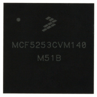
MCF5253CVM140 Freescale Semiconductor, MCF5253CVM140 Datasheet - Page 313

MCF5253CVM140
Manufacturer Part Number
MCF5253CVM140
Description
IC MPU 32BIT 140MHZ 225-MAPBGA
Manufacturer
Freescale Semiconductor
Series
MCF525xr
Datasheets
1.MCF5253VM140J.pdf
(34 pages)
2.MCF5253VM140J.pdf
(8 pages)
3.MCF5253VM140J.pdf
(648 pages)
4.MCF5253VM140J.pdf
(2 pages)
Specifications of MCF5253CVM140
Core Processor
Coldfire V2
Core Size
32-Bit
Speed
140MHz
Connectivity
CAN, EBI/EMI, I²C, QSPI, UART/USART, USB OTG
Peripherals
DMA, WDT
Program Memory Type
ROMless
Ram Size
128K x 8
Voltage - Supply (vcc/vdd)
1.08 V ~ 1.32 V
Data Converters
A/D 6x12b
Oscillator Type
External
Operating Temperature
-40°C ~ 85°C
Package / Case
225-MAPBGA
Family Name
MCF5xxx
Device Core
ColdFire V2
Device Core Size
32b
Frequency (max)
140MHz
Instruction Set Architecture
RISC
Supply Voltage 1 (typ)
1.2/3.3V
Operating Supply Voltage (max)
1.32/3.6V
Operating Supply Voltage (min)
1.08/3V
Operating Temp Range
-40C to 85C
Operating Temperature Classification
Industrial
Mounting
Surface Mount
Pin Count
225
Package Type
MA-BGA
Lead Free Status / RoHS Status
Lead free / RoHS Compliant
Number Of I /o
-
Eeprom Size
-
Program Memory Size
-
Lead Free Status / Rohs Status
Compliant
Available stocks
Company
Part Number
Manufacturer
Quantity
Price
Company:
Part Number:
MCF5253CVM140
Manufacturer:
FREESCALE
Quantity:
300
Company:
Part Number:
MCF5253CVM140
Manufacturer:
Freescale Semiconductor
Quantity:
10 000
Part Number:
MCF5253CVM140
Manufacturer:
FREESCALE
Quantity:
20 000
Company:
Part Number:
MCF5253CVM140J
Manufacturer:
Freescale Semiconductor
Quantity:
10 000
- MCF5253VM140J PDF datasheet
- MCF5253VM140J PDF datasheet #2
- MCF5253VM140J PDF datasheet #3
- MCF5253VM140J PDF datasheet #4
- Current page: 313 of 648
- Download datasheet (8Mb)
Figure 17-8
of the bit fields.
Freescale Semiconductor
1
2
3
4
5
6
7
8
9
10
11
12
U SOURCE SELECT
The IEC958 interface needs 64 * audio sample frequency clock for good operation. This is 2.822 MHz for operation at a
sample rate of 44.1 kHz.
When The IEC958 transmitter is set to follow SCLK1, SCLK2, SCLK3, or SCLK4, it will transmit at the same rate as the serial
audio interface only if the interface uses 64 bit clocks / word clock format.
When bit 11 is set, the FIFO is in its reset condition. The FIFO is always re-set to “contain 1 sample”. This sample value is
re-set at the same time to “all-zeros”.
U channel selection is described on section handling subcode processing.
Before starting IEC958 transmission to copy data from another incoming channel, first reset the FIFO to one sample
remaining, while the source selector is set to correct source. When the FIFO is switched to normal operation, transmission
will start normally.
Digital zero means data transmitted is digital zero, while “C” and “U” channel contain valid data. When digital zero is
transmitted, the IEC958 transmit FIFO is not read any more by the IEC958 transmit hardware.
PDOR1, PDOR2, PDOR3: Processor Data Out Register.
Reprogramming bits 15-12 during functional operation is not allowed. Reprogramming is only allowed while FIFO is in its
reset condition (bit 11 set ‘1’)
When “digital zero” is selected as a source, the FIFO outputs “zero” on its outgoing data bus, regardless of the input side and
content of the FIFO. No FIFO related exceptions are generated.
This bit controls the outgoing validity flag of the EBU transmitter. When it is re-set, all outgoing data is flagged as “valid”. If it
is set, all data is flagged “invalid”.
When the FIFO leaves the reset state, because the user write a “normal operation” state into the control register, the FIFO
is kept into reset until first long-word is written to it. As a result, the “start” of the normal operation is synchronized with
the writing of the first data into the FIFO.
This field selects what is output on EBUOUT1. If the field is “000,” the SPDIF output is off and outputs 0. If the field is “001”
to “100,” it muxes out one of the EBUIN’s to the EBUOUT, without any reformatting. When the field is set to “101,” this is
normal operation of the SPDIF transmitter.
Address MBAR2 + 0xD0 (Reset 0x3f00)
Field
1–0
Reset
Reset
illustrates the valid bits in the EBU2Config Register and
W
W
R
R
31
15
0
0
Table 17-6. EBU1Config Register Field Descriptions (continued)
30
14
0
0
00 No embedded U channel
01 U channel from IEC958 receive block. (CD mode)
10 Reserved, undefined
11 U channel from on-chip U channel transmitter.
29
13
0
1
28
12
0
1
27
11
Figure 17-8. EBU2Config Register
0
1
MCF5253 Reference Manual, Rev. 1
26
10
0
1
25
0
1
9
Description
24
0
1
8
IEC958 RECEIVE
SOUCE SELECT
23
0
0
7
22
0
0
6
Table 17-7
00
21
0
5
20
0
4
0
Access: User read/write
19
provides the description
0
0
3
Audio Interface Module (AIM)
18
0
0
2
00
17
0
0
1
Reset
16
0
0
0
4
Notes
17-15
Related parts for MCF5253CVM140
Image
Part Number
Description
Manufacturer
Datasheet
Request
R
Part Number:
Description:
Mcf5253 Coldfire? Microprocessor Data Sheet
Manufacturer:
Freescale Semiconductor, Inc
Datasheet:
Part Number:
Description:
Manufacturer:
Freescale Semiconductor, Inc
Datasheet:
Part Number:
Description:
Manufacturer:
Freescale Semiconductor, Inc
Datasheet:
Part Number:
Description:
Manufacturer:
Freescale Semiconductor, Inc
Datasheet:
Part Number:
Description:
Manufacturer:
Freescale Semiconductor, Inc
Datasheet:
Part Number:
Description:
Manufacturer:
Freescale Semiconductor, Inc
Datasheet:
Part Number:
Description:
Manufacturer:
Freescale Semiconductor, Inc
Datasheet:
Part Number:
Description:
Manufacturer:
Freescale Semiconductor, Inc
Datasheet:
Part Number:
Description:
Manufacturer:
Freescale Semiconductor, Inc
Datasheet:
Part Number:
Description:
Manufacturer:
Freescale Semiconductor, Inc
Datasheet:
Part Number:
Description:
Manufacturer:
Freescale Semiconductor, Inc
Datasheet:
Part Number:
Description:
Manufacturer:
Freescale Semiconductor, Inc
Datasheet:
Part Number:
Description:
Manufacturer:
Freescale Semiconductor, Inc
Datasheet:
Part Number:
Description:
Manufacturer:
Freescale Semiconductor, Inc
Datasheet:
Part Number:
Description:
Manufacturer:
Freescale Semiconductor, Inc
Datasheet:


