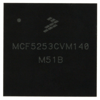
MCF5253CVM140 Freescale Semiconductor, MCF5253CVM140 Datasheet - Page 339

MCF5253CVM140
Manufacturer Part Number
MCF5253CVM140
Description
IC MPU 32BIT 140MHZ 225-MAPBGA
Manufacturer
Freescale Semiconductor
Series
MCF525xr
Datasheets
1.MCF5253VM140J.pdf
(34 pages)
2.MCF5253VM140J.pdf
(8 pages)
3.MCF5253VM140J.pdf
(648 pages)
4.MCF5253VM140J.pdf
(2 pages)
Specifications of MCF5253CVM140
Core Processor
Coldfire V2
Core Size
32-Bit
Speed
140MHz
Connectivity
CAN, EBI/EMI, I²C, QSPI, UART/USART, USB OTG
Peripherals
DMA, WDT
Program Memory Type
ROMless
Ram Size
128K x 8
Voltage - Supply (vcc/vdd)
1.08 V ~ 1.32 V
Data Converters
A/D 6x12b
Oscillator Type
External
Operating Temperature
-40°C ~ 85°C
Package / Case
225-MAPBGA
Family Name
MCF5xxx
Device Core
ColdFire V2
Device Core Size
32b
Frequency (max)
140MHz
Instruction Set Architecture
RISC
Supply Voltage 1 (typ)
1.2/3.3V
Operating Supply Voltage (max)
1.32/3.6V
Operating Supply Voltage (min)
1.08/3V
Operating Temp Range
-40C to 85C
Operating Temperature Classification
Industrial
Mounting
Surface Mount
Pin Count
225
Package Type
MA-BGA
Lead Free Status / RoHS Status
Lead free / RoHS Compliant
Number Of I /o
-
Eeprom Size
-
Program Memory Size
-
Lead Free Status / Rohs Status
Compliant
Available stocks
Company
Part Number
Manufacturer
Quantity
Price
Company:
Part Number:
MCF5253CVM140
Manufacturer:
FREESCALE
Quantity:
300
Company:
Part Number:
MCF5253CVM140
Manufacturer:
Freescale Semiconductor
Quantity:
10 000
Part Number:
MCF5253CVM140
Manufacturer:
FREESCALE
Quantity:
20 000
Company:
Part Number:
MCF5253CVM140J
Manufacturer:
Freescale Semiconductor
Quantity:
10 000
- MCF5253VM140J PDF datasheet
- MCF5253VM140J PDF datasheet #2
- MCF5253VM140J PDF datasheet #3
- MCF5253VM140J PDF datasheet #4
- Current page: 339 of 648
- Download datasheet (8Mb)
The block encoder works on the incoming PDOR3 stream. First, CRC insertion is done in the CRC
Calculate and Insert block (1), next the stream is scrambled in the Scramble block (2), and finally it is
byte-swapped in the Swap Bytes Block (3). All three operations can be configured by writing to the
blockControl register. CRC insertion and scrambling are done as described in CD Yellow Book.
The CRC insertion (1) and the Scrambling (2) are done on a block-by-block basis. A block is normally
2352 bytes long. A block starts after the so-called sync Pattern, “00FFFFFF-FFFFFFFF-FFFFFF00”. To
detect the start of a new block, two mechanisms are build into the encoder.
17.7.8.2
17.8
It is possible to use the DMA to transfer data to/from the FIFO’s in the audio interface module. However,
only PDIR2 and PDOR3 registers support DMA transfer, as the others need more than 1 long-word to
transfer data to/from the FIFO and cannot be used with DMA operation.
Operation is as follows:
Freescale Semiconductor
•
•
•
•
•
•
First long-word of a new block is assumed after finding the sync pattern
“00FFFFFF-FFFFFFFF-FFFFFF00”
First long-word of a new block is assumed exactly 2352 bytes after the first longword of the
previous block. This second detection mechanism builds in immunity for corrupted syncs. Even if
the sync is corrupted, the block encoder will correctly find the start of the a new block.
newBlock interrupt—Active when transmission of a new block is started. No direct
synchronization with data written to the transmit
noSync interrupt—Set when the sync pattern was not recognized for the current newBlock
interrupt.
ilSync interrupt—Set when the previous block did not have the correct length. (Length different
from 2352 bytes).
If PDIR2 is full and DMAConfig(1) is set to ‘0’, DMA1REQ is activated.
DMA Channel Interaction
CD-ROM Encoder Interrupts
Processor
Data
Sync
Recognition
Sync Settings
CRC
calculate
and
insert
4
MCF5253 Reference Manual, Rev. 1
Figure 17-22. Block Encoder
1
newBlockInt
ilSyncInt
noSyncInt
Scramble
On/Off select
FIFO
2
.
Swap select
Swap
Bytes
3
To
audio
data
bus
Audio Interface Module (AIM)
17-41
Related parts for MCF5253CVM140
Image
Part Number
Description
Manufacturer
Datasheet
Request
R
Part Number:
Description:
Mcf5253 Coldfire? Microprocessor Data Sheet
Manufacturer:
Freescale Semiconductor, Inc
Datasheet:
Part Number:
Description:
Manufacturer:
Freescale Semiconductor, Inc
Datasheet:
Part Number:
Description:
Manufacturer:
Freescale Semiconductor, Inc
Datasheet:
Part Number:
Description:
Manufacturer:
Freescale Semiconductor, Inc
Datasheet:
Part Number:
Description:
Manufacturer:
Freescale Semiconductor, Inc
Datasheet:
Part Number:
Description:
Manufacturer:
Freescale Semiconductor, Inc
Datasheet:
Part Number:
Description:
Manufacturer:
Freescale Semiconductor, Inc
Datasheet:
Part Number:
Description:
Manufacturer:
Freescale Semiconductor, Inc
Datasheet:
Part Number:
Description:
Manufacturer:
Freescale Semiconductor, Inc
Datasheet:
Part Number:
Description:
Manufacturer:
Freescale Semiconductor, Inc
Datasheet:
Part Number:
Description:
Manufacturer:
Freescale Semiconductor, Inc
Datasheet:
Part Number:
Description:
Manufacturer:
Freescale Semiconductor, Inc
Datasheet:
Part Number:
Description:
Manufacturer:
Freescale Semiconductor, Inc
Datasheet:
Part Number:
Description:
Manufacturer:
Freescale Semiconductor, Inc
Datasheet:
Part Number:
Description:
Manufacturer:
Freescale Semiconductor, Inc
Datasheet:


