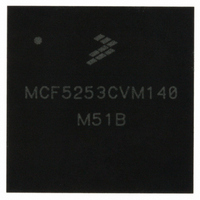
MCF5253CVM140 Freescale Semiconductor, MCF5253CVM140 Datasheet - Page 201

MCF5253CVM140
Manufacturer Part Number
MCF5253CVM140
Description
IC MPU 32BIT 140MHZ 225-MAPBGA
Manufacturer
Freescale Semiconductor
Series
MCF525xr
Datasheets
1.MCF5253VM140J.pdf
(34 pages)
2.MCF5253VM140J.pdf
(8 pages)
3.MCF5253VM140J.pdf
(648 pages)
4.MCF5253VM140J.pdf
(2 pages)
Specifications of MCF5253CVM140
Core Processor
Coldfire V2
Core Size
32-Bit
Speed
140MHz
Connectivity
CAN, EBI/EMI, I²C, QSPI, UART/USART, USB OTG
Peripherals
DMA, WDT
Program Memory Type
ROMless
Ram Size
128K x 8
Voltage - Supply (vcc/vdd)
1.08 V ~ 1.32 V
Data Converters
A/D 6x12b
Oscillator Type
External
Operating Temperature
-40°C ~ 85°C
Package / Case
225-MAPBGA
Family Name
MCF5xxx
Device Core
ColdFire V2
Device Core Size
32b
Frequency (max)
140MHz
Instruction Set Architecture
RISC
Supply Voltage 1 (typ)
1.2/3.3V
Operating Supply Voltage (max)
1.32/3.6V
Operating Supply Voltage (min)
1.08/3V
Operating Temp Range
-40C to 85C
Operating Temperature Classification
Industrial
Mounting
Surface Mount
Pin Count
225
Package Type
MA-BGA
Lead Free Status / RoHS Status
Lead free / RoHS Compliant
Number Of I /o
-
Eeprom Size
-
Program Memory Size
-
Lead Free Status / Rohs Status
Compliant
Available stocks
Company
Part Number
Manufacturer
Quantity
Price
Company:
Part Number:
MCF5253CVM140
Manufacturer:
FREESCALE
Quantity:
300
Company:
Part Number:
MCF5253CVM140
Manufacturer:
Freescale Semiconductor
Quantity:
10 000
Part Number:
MCF5253CVM140
Manufacturer:
FREESCALE
Quantity:
20 000
Company:
Part Number:
MCF5253CVM140J
Manufacturer:
Freescale Semiconductor
Quantity:
10 000
- MCF5253VM140J PDF datasheet
- MCF5253VM140J PDF datasheet #2
- MCF5253VM140J PDF datasheet #3
- MCF5253VM140J PDF datasheet #4
- Current page: 201 of 648
- Download datasheet (8Mb)
To support this bus set-up, a number of signals are available.
The extra bus signals, and their configuration are detailed in the following section.
13.1.1
Buffer enables BUFENB1 and BUFENB2 allow a seamless interface to external bus buffers. The buffers
are placed on the address and the data bus.
As shown in
before the falling edge of the Chip Select signal, and continue to be active for a time CSPOST after the
rising edge of the chip select signal. The pre-drive time CSPRE is realized by delaying the falling edge of
the select signal. If pre-drive time CSPRE is programmed non-zero, and internal ColdFire cycle
termination is used, chip select length will be CSPRE shorter than the programmed length. Times CSPRE,
CSPOST are the same for both BUFENB1 AND BUFENB2. Times CSPRE, CSPOST are independently
programmable for every Chip Select.
Buffer enable configuration is programmable using the IDE_CONFIG1 register.
Freescale Semiconductor
•
•
•
•
•
BUFENB1—active-low external buffer enable. This enable is always active when the CS0/CS4
pin is active, and should enable a buffer going to the external boot Flash / ROM and any additional
memories or controllers.
When CS0 is being used internally as the Chip Select for the boot ROM, the CS0/CS4 pin operates
with the CS4 settings, BUFENB1 settings then apply to CS4.
BUFENB2—active-low external buffer enable. This enable is always inactive when the CS0/CS4
pin is active, and should enable a buffer for the IDE / SmartMedia Interface.
IDE_DIOR, IDE_DIOW—active-low IDE bus read and write strobe can also be used to implement
a SmartMedia interface.
IDE_IORDY—active-high “ready” indication from IDE device to MCF5253.
CS0, CS1,
DIOR, DIOW, SRE, SWE
Buffer Enables BUFENB1, BUFENB2, and Associated Logic
Figure
Either of the buffer enables can be programmed to be active on CS1 or CS2
13-2, the buffer enables BUFENB1 and BUFENB2 will go active at time CSPRE
CSx_core
BUFENBx
bufenx_b
Figure 13-2. Buffer Enables (BUFENB1 and BUFENB2)
MCF5253 Reference Manual, Rev. 1
CSPRE
cspre
NOTE
CSPOST
cspost
IDE and Flash Media Interface
13-3
Related parts for MCF5253CVM140
Image
Part Number
Description
Manufacturer
Datasheet
Request
R
Part Number:
Description:
Mcf5253 Coldfire? Microprocessor Data Sheet
Manufacturer:
Freescale Semiconductor, Inc
Datasheet:
Part Number:
Description:
Manufacturer:
Freescale Semiconductor, Inc
Datasheet:
Part Number:
Description:
Manufacturer:
Freescale Semiconductor, Inc
Datasheet:
Part Number:
Description:
Manufacturer:
Freescale Semiconductor, Inc
Datasheet:
Part Number:
Description:
Manufacturer:
Freescale Semiconductor, Inc
Datasheet:
Part Number:
Description:
Manufacturer:
Freescale Semiconductor, Inc
Datasheet:
Part Number:
Description:
Manufacturer:
Freescale Semiconductor, Inc
Datasheet:
Part Number:
Description:
Manufacturer:
Freescale Semiconductor, Inc
Datasheet:
Part Number:
Description:
Manufacturer:
Freescale Semiconductor, Inc
Datasheet:
Part Number:
Description:
Manufacturer:
Freescale Semiconductor, Inc
Datasheet:
Part Number:
Description:
Manufacturer:
Freescale Semiconductor, Inc
Datasheet:
Part Number:
Description:
Manufacturer:
Freescale Semiconductor, Inc
Datasheet:
Part Number:
Description:
Manufacturer:
Freescale Semiconductor, Inc
Datasheet:
Part Number:
Description:
Manufacturer:
Freescale Semiconductor, Inc
Datasheet:
Part Number:
Description:
Manufacturer:
Freescale Semiconductor, Inc
Datasheet:


