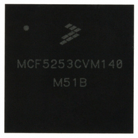
MCF5253CVM140 Freescale Semiconductor, MCF5253CVM140 Datasheet - Page 405

MCF5253CVM140
Manufacturer Part Number
MCF5253CVM140
Description
IC MPU 32BIT 140MHZ 225-MAPBGA
Manufacturer
Freescale Semiconductor
Series
MCF525xr
Datasheets
1.MCF5253VM140J.pdf
(34 pages)
2.MCF5253VM140J.pdf
(8 pages)
3.MCF5253VM140J.pdf
(648 pages)
4.MCF5253VM140J.pdf
(2 pages)
Specifications of MCF5253CVM140
Core Processor
Coldfire V2
Core Size
32-Bit
Speed
140MHz
Connectivity
CAN, EBI/EMI, I²C, QSPI, UART/USART, USB OTG
Peripherals
DMA, WDT
Program Memory Type
ROMless
Ram Size
128K x 8
Voltage - Supply (vcc/vdd)
1.08 V ~ 1.32 V
Data Converters
A/D 6x12b
Oscillator Type
External
Operating Temperature
-40°C ~ 85°C
Package / Case
225-MAPBGA
Family Name
MCF5xxx
Device Core
ColdFire V2
Device Core Size
32b
Frequency (max)
140MHz
Instruction Set Architecture
RISC
Supply Voltage 1 (typ)
1.2/3.3V
Operating Supply Voltage (max)
1.32/3.6V
Operating Supply Voltage (min)
1.08/3V
Operating Temp Range
-40C to 85C
Operating Temperature Classification
Industrial
Mounting
Surface Mount
Pin Count
225
Package Type
MA-BGA
Lead Free Status / RoHS Status
Lead free / RoHS Compliant
Number Of I /o
-
Eeprom Size
-
Program Memory Size
-
Lead Free Status / Rohs Status
Compliant
Available stocks
Company
Part Number
Manufacturer
Quantity
Price
Company:
Part Number:
MCF5253CVM140
Manufacturer:
FREESCALE
Quantity:
300
Company:
Part Number:
MCF5253CVM140
Manufacturer:
Freescale Semiconductor
Quantity:
10 000
Part Number:
MCF5253CVM140
Manufacturer:
FREESCALE
Quantity:
20 000
Company:
Part Number:
MCF5253CVM140J
Manufacturer:
Freescale Semiconductor
Quantity:
10 000
- MCF5253VM140J PDF datasheet
- MCF5253VM140J PDF datasheet #2
- MCF5253VM140J PDF datasheet #3
- MCF5253VM140J PDF datasheet #4
- Current page: 405 of 648
- Download datasheet (8Mb)
20.5.5
The TDR configures the operation of the hardware breakpoint logic within the debug module and controls
the actions taken under the defined conditions. The breakpoint logic may be configured as a one- or
two-level trigger, where bits [31:16] of the TDR define the 2nd level trigger and bits [15:0] define the first
level trigger. The TDR is accessible in supervisor mode as debug control register $7 using the WDEBUG
instruction and through the BDM port using the WDMREG command.
Freescale Semiconductor
.
31–29
Field
TRC
TDR
TDR
Reset
Reset
15
14
W
W
R
R
The trigger response control determines how the processor is to respond to a completed trigger condition. The
trigger response is always displayed on the DDATA pins.
00 Display on DDATA only
01 Processor halt
10 Debug interrupt
11 Reserved
0 Level-2 trigger = PC_condition & Address_range & Data_condition
1 Level-2 trigger = PC_condition | (Address_range & Data_condition)
0 Level-1 trigger = PC_condition & Address_range & Data_condition
1 Level-1 trigger = PC_condition | (Address_range & Data_condition)
31
15
–
–
Trigger Definition Register (TDR)
TRC
30
14
–
–
Table 20-21. Trigger Definition Register (TDR) Field Descriptions
Address[1:0]
EBL
29
13
–
–
00
01
10
11
0x
1x
xx
EDLW
EDLW
Table 20-20. Access and Operand Data Location
28
12
–
–
Figure 20-36. Trigger Definition Register (TDR)
EDWL
EDWL
27
11
–
–
MCF5253 Reference Manual, Rev. 1
EDWU
EDWU
26
10
–
–
Access Size
Word
Word
Long
Byte
Byte
Byte
Byte
EDLL
EDLL
25
–
–
9
EDLM
EDLM
Description
24
–
–
8
EDUM
EDUM
23
–
–
7
EDUU
EDUU
Operand Location
22
–
–
6
Data[31:24]
Data[23:16]
Data[31:16]
Data[15:8]
Data[15:0]
Data[31:0]
Data[7:0]
21
DI
DI
–
–
5
Background Debug Mode (BDM) Interface
EAI
EAI
20
–
–
4
EAR
EAR
19
–
–
3
Access: User write only
EAL
EAL
18
–
2
–
EPC
EPC
17
–
–
1
20-35
PCI
PCI
16
–
–
0
Related parts for MCF5253CVM140
Image
Part Number
Description
Manufacturer
Datasheet
Request
R
Part Number:
Description:
Mcf5253 Coldfire? Microprocessor Data Sheet
Manufacturer:
Freescale Semiconductor, Inc
Datasheet:
Part Number:
Description:
Manufacturer:
Freescale Semiconductor, Inc
Datasheet:
Part Number:
Description:
Manufacturer:
Freescale Semiconductor, Inc
Datasheet:
Part Number:
Description:
Manufacturer:
Freescale Semiconductor, Inc
Datasheet:
Part Number:
Description:
Manufacturer:
Freescale Semiconductor, Inc
Datasheet:
Part Number:
Description:
Manufacturer:
Freescale Semiconductor, Inc
Datasheet:
Part Number:
Description:
Manufacturer:
Freescale Semiconductor, Inc
Datasheet:
Part Number:
Description:
Manufacturer:
Freescale Semiconductor, Inc
Datasheet:
Part Number:
Description:
Manufacturer:
Freescale Semiconductor, Inc
Datasheet:
Part Number:
Description:
Manufacturer:
Freescale Semiconductor, Inc
Datasheet:
Part Number:
Description:
Manufacturer:
Freescale Semiconductor, Inc
Datasheet:
Part Number:
Description:
Manufacturer:
Freescale Semiconductor, Inc
Datasheet:
Part Number:
Description:
Manufacturer:
Freescale Semiconductor, Inc
Datasheet:
Part Number:
Description:
Manufacturer:
Freescale Semiconductor, Inc
Datasheet:
Part Number:
Description:
Manufacturer:
Freescale Semiconductor, Inc
Datasheet:


