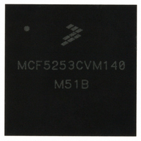
MCF5253CVM140 Freescale Semiconductor, MCF5253CVM140 Datasheet - Page 146

MCF5253CVM140
Manufacturer Part Number
MCF5253CVM140
Description
IC MPU 32BIT 140MHZ 225-MAPBGA
Manufacturer
Freescale Semiconductor
Series
MCF525xr
Datasheets
1.MCF5253VM140J.pdf
(34 pages)
2.MCF5253VM140J.pdf
(8 pages)
3.MCF5253VM140J.pdf
(648 pages)
4.MCF5253VM140J.pdf
(2 pages)
Specifications of MCF5253CVM140
Core Processor
Coldfire V2
Core Size
32-Bit
Speed
140MHz
Connectivity
CAN, EBI/EMI, I²C, QSPI, UART/USART, USB OTG
Peripherals
DMA, WDT
Program Memory Type
ROMless
Ram Size
128K x 8
Voltage - Supply (vcc/vdd)
1.08 V ~ 1.32 V
Data Converters
A/D 6x12b
Oscillator Type
External
Operating Temperature
-40°C ~ 85°C
Package / Case
225-MAPBGA
Family Name
MCF5xxx
Device Core
ColdFire V2
Device Core Size
32b
Frequency (max)
140MHz
Instruction Set Architecture
RISC
Supply Voltage 1 (typ)
1.2/3.3V
Operating Supply Voltage (max)
1.32/3.6V
Operating Supply Voltage (min)
1.08/3V
Operating Temp Range
-40C to 85C
Operating Temperature Classification
Industrial
Mounting
Surface Mount
Pin Count
225
Package Type
MA-BGA
Lead Free Status / RoHS Status
Lead free / RoHS Compliant
Number Of I /o
-
Eeprom Size
-
Program Memory Size
-
Lead Free Status / Rohs Status
Compliant
Available stocks
Company
Part Number
Manufacturer
Quantity
Price
Company:
Part Number:
MCF5253CVM140
Manufacturer:
FREESCALE
Quantity:
300
Company:
Part Number:
MCF5253CVM140
Manufacturer:
Freescale Semiconductor
Quantity:
10 000
Part Number:
MCF5253CVM140
Manufacturer:
FREESCALE
Quantity:
20 000
Company:
Part Number:
MCF5253CVM140J
Manufacturer:
Freescale Semiconductor
Quantity:
10 000
- MCF5253VM140J PDF datasheet
- MCF5253VM140J PDF datasheet #2
- MCF5253VM140J PDF datasheet #3
- MCF5253VM140J PDF datasheet #4
- Current page: 146 of 648
- Download datasheet (8Mb)
System Integration Module (SIM)
9.2.1
Table 9-2
memory-mapped registers offset from the MBAR or MBAR2 address pointers. The following should be
noted when programming the MBAR registers:
9-2
MBAR + $00C
MBAR + $01C
MBAR + $02C
MBAR + $03C
MBAR + $04C
MBAR + $000
MBAR + $004
MBAR + $008
MBAR + $010
MBAR + $014
MBAR + $018
MBAR + $020
MBAR + $024
MBAR + $028
MBAR + $030
MBAR + $034
MBAR + $038
MBAR + $040
MBAR + $044
MBAR + $050
•
•
Address
The Module Base Address Registers are accessed in supervisor mode only using the MOVEC
instruction.
The MBAR and MBAR2 are accessible using the debug module as read/write registers. See
Chapter 20, “Background Debug Mode (BDM) Interface,”
shows the memory map of all the SIM registers. The internal registers in the SIM are
SIM Register Memory Map
SYSTEM CONTROL REG
BUS MASTER CONTROL REG
Primary interrupt Pending Reg
Primary Interrupt Mask Reg
Primary Interrupt Control Reg
Primary Interrupt Control Reg
CPU + $C0F
CPU + $C0E
Address
Description
Table 9-1. MBAR Register Addresses
MBAR2
MBAR
Name
MCF5253 Reference Manual, Rev. 1
–
–
–
–
–
–
–
–
–
–
–
–
–
–
Table 9-2. SIM Memory Map
(Bytes)
Size
4
4
Module base address register
Module base address register 2
RSR
Reserved
Reserved
MPARK
Reserved
IPR
IMR
ICR0
ICR4
0
Description
for more details.
Reserved
SYPCR
ICR1
ICR5
1
SWIVR
ICR2
ICR6
Freescale Semiconductor
2
SWSR
ICR3
ICR7
3
Related parts for MCF5253CVM140
Image
Part Number
Description
Manufacturer
Datasheet
Request
R
Part Number:
Description:
Mcf5253 Coldfire? Microprocessor Data Sheet
Manufacturer:
Freescale Semiconductor, Inc
Datasheet:
Part Number:
Description:
Manufacturer:
Freescale Semiconductor, Inc
Datasheet:
Part Number:
Description:
Manufacturer:
Freescale Semiconductor, Inc
Datasheet:
Part Number:
Description:
Manufacturer:
Freescale Semiconductor, Inc
Datasheet:
Part Number:
Description:
Manufacturer:
Freescale Semiconductor, Inc
Datasheet:
Part Number:
Description:
Manufacturer:
Freescale Semiconductor, Inc
Datasheet:
Part Number:
Description:
Manufacturer:
Freescale Semiconductor, Inc
Datasheet:
Part Number:
Description:
Manufacturer:
Freescale Semiconductor, Inc
Datasheet:
Part Number:
Description:
Manufacturer:
Freescale Semiconductor, Inc
Datasheet:
Part Number:
Description:
Manufacturer:
Freescale Semiconductor, Inc
Datasheet:
Part Number:
Description:
Manufacturer:
Freescale Semiconductor, Inc
Datasheet:
Part Number:
Description:
Manufacturer:
Freescale Semiconductor, Inc
Datasheet:
Part Number:
Description:
Manufacturer:
Freescale Semiconductor, Inc
Datasheet:
Part Number:
Description:
Manufacturer:
Freescale Semiconductor, Inc
Datasheet:
Part Number:
Description:
Manufacturer:
Freescale Semiconductor, Inc
Datasheet:


