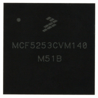
MCF5253CVM140 Freescale Semiconductor, MCF5253CVM140 Datasheet - Page 196

MCF5253CVM140
Manufacturer Part Number
MCF5253CVM140
Description
IC MPU 32BIT 140MHZ 225-MAPBGA
Manufacturer
Freescale Semiconductor
Series
MCF525xr
Datasheets
1.MCF5253VM140J.pdf
(34 pages)
2.MCF5253VM140J.pdf
(8 pages)
3.MCF5253VM140J.pdf
(648 pages)
4.MCF5253VM140J.pdf
(2 pages)
Specifications of MCF5253CVM140
Core Processor
Coldfire V2
Core Size
32-Bit
Speed
140MHz
Connectivity
CAN, EBI/EMI, I²C, QSPI, UART/USART, USB OTG
Peripherals
DMA, WDT
Program Memory Type
ROMless
Ram Size
128K x 8
Voltage - Supply (vcc/vdd)
1.08 V ~ 1.32 V
Data Converters
A/D 6x12b
Oscillator Type
External
Operating Temperature
-40°C ~ 85°C
Package / Case
225-MAPBGA
Family Name
MCF5xxx
Device Core
ColdFire V2
Device Core Size
32b
Frequency (max)
140MHz
Instruction Set Architecture
RISC
Supply Voltage 1 (typ)
1.2/3.3V
Operating Supply Voltage (max)
1.32/3.6V
Operating Supply Voltage (min)
1.08/3V
Operating Temp Range
-40C to 85C
Operating Temperature Classification
Industrial
Mounting
Surface Mount
Pin Count
225
Package Type
MA-BGA
Lead Free Status / RoHS Status
Lead free / RoHS Compliant
Number Of I /o
-
Eeprom Size
-
Program Memory Size
-
Lead Free Status / Rohs Status
Compliant
Available stocks
Company
Part Number
Manufacturer
Quantity
Price
Company:
Part Number:
MCF5253CVM140
Manufacturer:
FREESCALE
Quantity:
300
Company:
Part Number:
MCF5253CVM140
Manufacturer:
Freescale Semiconductor
Quantity:
10 000
Part Number:
MCF5253CVM140
Manufacturer:
FREESCALE
Quantity:
20 000
Company:
Part Number:
MCF5253CVM140J
Manufacturer:
Freescale Semiconductor
Quantity:
10 000
- MCF5253VM140J PDF datasheet
- MCF5253VM140J PDF datasheet #2
- MCF5253VM140J PDF datasheet #3
- MCF5253VM140J PDF datasheet #4
- Current page: 196 of 648
- Download datasheet (8Mb)
Analog to Digital Converter (ADC)
12.4
Each ADC input channel has its own on-chip comparator the output of which is multiplexed with the
digital section.The reason to have separate comparators for each channel allows for the inputs to be used
as GPI’s. In this mode the ADREF should be a fixed level (typically VDD/2) and each comparator is then
being used to indicate if its input is above or below this reference (HIGH or LOW). The state of each GPI
in this case is read using the GPIO_READ registers.
The ADC uses the sigma-delta modulation principle. The ADC external components required are an
integrator circuit comprising of a resistor and capacitor. The desired values for this integrator network are
dependent on the BUSCLK clock frequency and the associated setting of the ADconfig[ADCLK_SEL]
bits, which determine the maximum ADOUT PWM frequency.
12.4.1
Do not run the ADC clock any faster than 10 MHz. This results in a maximum sampling frequency of
2441 Hz (10 MHz/4096).
To calculate the external component values use the following equation:
where K is a constant. If K is small, the ripple on the comparator input will be quite large, and there will
be some mis-measurement because the average value on both comparator pins is not equal. If K is small,
12-4
ADVALUE
15–13
Field
11–0
OF
12
Functional Description
Recommendations to Set-up of ADC and External Components
It is possible to mix the use of each of these inputs between ADC and GPI
function as the ADOUT/SCLK4/GPIO58 pin can be switched between
providing the ramping ADOUT signal (ADC mode) to providing a fixed
level (VDD/2) by switching its operation to SCLK4 mode when
appropriate. SCLK4 will output a 50% duty cycle clock. Which when
integrated will produce a reference voltage close to VDD/2. The output
frequency of SCLK4 can be varied by programming the IIS4 Audio register.
See
Descriptions.”
Reserved, should be cleared.
Overflow. Indicates the input voltage is out of range. The ADC block does not support full rail-to-rail
conversions.
0 No overflow condition.
1 Overflow. Input signal is outside the operating voltage range of the ADC.
AD measurement result.
Section 17.5, “Serial Audio Interface (I2S/EIAJ) Register
Table 12-3. ADvalue Register Field Descriptions
MCF5253 Reference Manual, Rev. 1
RC
=
K
NOTE
×
t
Description
Freescale Semiconductor
Eqn. 12-1
Related parts for MCF5253CVM140
Image
Part Number
Description
Manufacturer
Datasheet
Request
R
Part Number:
Description:
Mcf5253 Coldfire? Microprocessor Data Sheet
Manufacturer:
Freescale Semiconductor, Inc
Datasheet:
Part Number:
Description:
Manufacturer:
Freescale Semiconductor, Inc
Datasheet:
Part Number:
Description:
Manufacturer:
Freescale Semiconductor, Inc
Datasheet:
Part Number:
Description:
Manufacturer:
Freescale Semiconductor, Inc
Datasheet:
Part Number:
Description:
Manufacturer:
Freescale Semiconductor, Inc
Datasheet:
Part Number:
Description:
Manufacturer:
Freescale Semiconductor, Inc
Datasheet:
Part Number:
Description:
Manufacturer:
Freescale Semiconductor, Inc
Datasheet:
Part Number:
Description:
Manufacturer:
Freescale Semiconductor, Inc
Datasheet:
Part Number:
Description:
Manufacturer:
Freescale Semiconductor, Inc
Datasheet:
Part Number:
Description:
Manufacturer:
Freescale Semiconductor, Inc
Datasheet:
Part Number:
Description:
Manufacturer:
Freescale Semiconductor, Inc
Datasheet:
Part Number:
Description:
Manufacturer:
Freescale Semiconductor, Inc
Datasheet:
Part Number:
Description:
Manufacturer:
Freescale Semiconductor, Inc
Datasheet:
Part Number:
Description:
Manufacturer:
Freescale Semiconductor, Inc
Datasheet:
Part Number:
Description:
Manufacturer:
Freescale Semiconductor, Inc
Datasheet:


