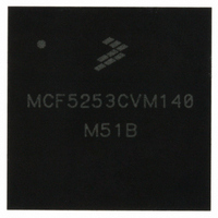
MCF5253CVM140 Freescale Semiconductor, MCF5253CVM140 Datasheet - Page 378

MCF5253CVM140
Manufacturer Part Number
MCF5253CVM140
Description
IC MPU 32BIT 140MHZ 225-MAPBGA
Manufacturer
Freescale Semiconductor
Series
MCF525xr
Datasheets
1.MCF5253VM140J.pdf
(34 pages)
2.MCF5253VM140J.pdf
(8 pages)
3.MCF5253VM140J.pdf
(648 pages)
4.MCF5253VM140J.pdf
(2 pages)
Specifications of MCF5253CVM140
Core Processor
Coldfire V2
Core Size
32-Bit
Speed
140MHz
Connectivity
CAN, EBI/EMI, I²C, QSPI, UART/USART, USB OTG
Peripherals
DMA, WDT
Program Memory Type
ROMless
Ram Size
128K x 8
Voltage - Supply (vcc/vdd)
1.08 V ~ 1.32 V
Data Converters
A/D 6x12b
Oscillator Type
External
Operating Temperature
-40°C ~ 85°C
Package / Case
225-MAPBGA
Family Name
MCF5xxx
Device Core
ColdFire V2
Device Core Size
32b
Frequency (max)
140MHz
Instruction Set Architecture
RISC
Supply Voltage 1 (typ)
1.2/3.3V
Operating Supply Voltage (max)
1.32/3.6V
Operating Supply Voltage (min)
1.08/3V
Operating Temp Range
-40C to 85C
Operating Temperature Classification
Industrial
Mounting
Surface Mount
Pin Count
225
Package Type
MA-BGA
Lead Free Status / RoHS Status
Lead free / RoHS Compliant
Number Of I /o
-
Eeprom Size
-
Program Memory Size
-
Lead Free Status / Rohs Status
Compliant
Available stocks
Company
Part Number
Manufacturer
Quantity
Price
Company:
Part Number:
MCF5253CVM140
Manufacturer:
FREESCALE
Quantity:
300
Company:
Part Number:
MCF5253CVM140
Manufacturer:
Freescale Semiconductor
Quantity:
10 000
Part Number:
MCF5253CVM140
Manufacturer:
FREESCALE
Quantity:
20 000
Company:
Part Number:
MCF5253CVM140J
Manufacturer:
Freescale Semiconductor
Quantity:
10 000
- MCF5253VM140J PDF datasheet
- MCF5253VM140J PDF datasheet #2
- MCF5253VM140J PDF datasheet #3
- MCF5253VM140J PDF datasheet #4
- Current page: 378 of 648
- Download datasheet (8Mb)
Background Debug Mode (BDM) Interface
was loaded, then the GO command simply causes the processor to exit the halted state and pass control to
the instruction address contained in the PC.
ColdFire also handles a special case of the assertion of BKPT while the processor is stopped by execution
of the STOP instruction. For this case, the processor exits the stopped mode and enters the halted state.
Once halted, all BDM commands may be exercised. When the processor is restarted, it continues with the
execution of the next sequential instruction. For example, the instruction following the STOP opcode.
The halt source is indicated in CSR[27:24]. For simultaneous halt conditions, the highest priority source
is indicated.
20.3.2
Once the CPU is halted and the halt status reflected on the PST outputs, the development system may send
unrestricted commands to the debug module. The debug module implements a synchronous protocol using
a three-pin interface: development serial clock (DSCLK), development serial input (DSI), and
development serial output (DSO). The development system serves as the serial communication channel
master and is responsible for generation of the clock (DSCLK). The maximum operating bandwidth of the
serial channel is DC to 1/5 of the processor frequency. The channel uses a full duplex mode, where data is
transmitted and received simultaneously by both master and slave devices. The transmission consists of
17-bit packets composed of a status/control bit and a 16-bit data word. As shown in
transitions are enabled on a rising edge of the processor clock when DSCLK is high. For example, DSI is
sampled and DSO is driven. The DSCLK signal must also be sampled low (on a positive edge of
CPUCLK) between each bit exchange. The MSB is transferred first.
Both DSCLK and DSI are synchronized inputs.The DSCLK signal essentially acts as a pseudo “clock
enable” and is sampled on the rising edge of CPUCLK as well as the DSI. The DSO output is delayed from
the DSCLK-enabled CPUCLK rising edge. All events in the debug module’s serial state machine are based
on the rising edge of the microprocessor clock.
20-8
BDM Serial Interface
In this case, the normal reset exception processing is bypassed. Conversely,
if the PC register was not loaded, then the GO command causes the
processor to exit the halted state and continue with reset exception
processing.
Figure 20-3. BDM Serial Transfer
MCF5253 Reference Manual, Rev. 1
NOTE
Figure
Freescale Semiconductor
20-3, all state
Related parts for MCF5253CVM140
Image
Part Number
Description
Manufacturer
Datasheet
Request
R
Part Number:
Description:
Mcf5253 Coldfire? Microprocessor Data Sheet
Manufacturer:
Freescale Semiconductor, Inc
Datasheet:
Part Number:
Description:
Manufacturer:
Freescale Semiconductor, Inc
Datasheet:
Part Number:
Description:
Manufacturer:
Freescale Semiconductor, Inc
Datasheet:
Part Number:
Description:
Manufacturer:
Freescale Semiconductor, Inc
Datasheet:
Part Number:
Description:
Manufacturer:
Freescale Semiconductor, Inc
Datasheet:
Part Number:
Description:
Manufacturer:
Freescale Semiconductor, Inc
Datasheet:
Part Number:
Description:
Manufacturer:
Freescale Semiconductor, Inc
Datasheet:
Part Number:
Description:
Manufacturer:
Freescale Semiconductor, Inc
Datasheet:
Part Number:
Description:
Manufacturer:
Freescale Semiconductor, Inc
Datasheet:
Part Number:
Description:
Manufacturer:
Freescale Semiconductor, Inc
Datasheet:
Part Number:
Description:
Manufacturer:
Freescale Semiconductor, Inc
Datasheet:
Part Number:
Description:
Manufacturer:
Freescale Semiconductor, Inc
Datasheet:
Part Number:
Description:
Manufacturer:
Freescale Semiconductor, Inc
Datasheet:
Part Number:
Description:
Manufacturer:
Freescale Semiconductor, Inc
Datasheet:
Part Number:
Description:
Manufacturer:
Freescale Semiconductor, Inc
Datasheet:


