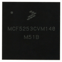
MCF5253CVM140 Freescale Semiconductor, MCF5253CVM140 Datasheet - Page 425

MCF5253CVM140
Manufacturer Part Number
MCF5253CVM140
Description
IC MPU 32BIT 140MHZ 225-MAPBGA
Manufacturer
Freescale Semiconductor
Series
MCF525xr
Datasheets
1.MCF5253VM140J.pdf
(34 pages)
2.MCF5253VM140J.pdf
(8 pages)
3.MCF5253VM140J.pdf
(648 pages)
4.MCF5253VM140J.pdf
(2 pages)
Specifications of MCF5253CVM140
Core Processor
Coldfire V2
Core Size
32-Bit
Speed
140MHz
Connectivity
CAN, EBI/EMI, I²C, QSPI, UART/USART, USB OTG
Peripherals
DMA, WDT
Program Memory Type
ROMless
Ram Size
128K x 8
Voltage - Supply (vcc/vdd)
1.08 V ~ 1.32 V
Data Converters
A/D 6x12b
Oscillator Type
External
Operating Temperature
-40°C ~ 85°C
Package / Case
225-MAPBGA
Family Name
MCF5xxx
Device Core
ColdFire V2
Device Core Size
32b
Frequency (max)
140MHz
Instruction Set Architecture
RISC
Supply Voltage 1 (typ)
1.2/3.3V
Operating Supply Voltage (max)
1.32/3.6V
Operating Supply Voltage (min)
1.08/3V
Operating Temp Range
-40C to 85C
Operating Temperature Classification
Industrial
Mounting
Surface Mount
Pin Count
225
Package Type
MA-BGA
Lead Free Status / RoHS Status
Lead free / RoHS Compliant
Number Of I /o
-
Eeprom Size
-
Program Memory Size
-
Lead Free Status / Rohs Status
Compliant
Available stocks
Company
Part Number
Manufacturer
Quantity
Price
Company:
Part Number:
MCF5253CVM140
Manufacturer:
FREESCALE
Quantity:
300
Company:
Part Number:
MCF5253CVM140
Manufacturer:
Freescale Semiconductor
Quantity:
10 000
Part Number:
MCF5253CVM140
Manufacturer:
FREESCALE
Quantity:
20 000
Company:
Part Number:
MCF5253CVM140J
Manufacturer:
Freescale Semiconductor
Quantity:
10 000
- MCF5253VM140J PDF datasheet
- MCF5253VM140J PDF datasheet #2
- MCF5253VM140J PDF datasheet #3
- MCF5253VM140J PDF datasheet #4
- Current page: 425 of 648
- Download datasheet (8Mb)
The 16 kbyte SRAM is connected via an arbiter to 3 busses:
The ATA controller has 2 busses, one connected to the internal bus, the second connected to the local ATA
DMA engine. The USB and ATA DMA controller are connected to the internal bus. For both, this
connection is used to access the module registers. All USB data transfers initiated by the USB will be to
and from the 16 kbytes cache memory. The USB does not see any other memory on the device.
22.3.1.1
The USB controller is little-endian, while the CPU is big-endian. The ATA controller endianness is
programmable; It can operate in both little-endian and big-endian modes. To resolve the issue, the cache
memory is visible from the CPU in straight-endianess and in swapped-endianness mode.
22.3.1.2
The DMA of the ATA block can be used to transfer data between the ATA module and the cache RAM. In
order to transfer data between these two blocks, proceed as follows:
Freescale Semiconductor
•
•
•
1. Make sure no unwanted transfer will start when configuring the DMA by clearing the
2. Program bit MISCCR[DMAEND] to correctly reflect the endianness on the DMA you need.
3. Program ATA_DADDR[ATAADDR] to contain the address in the ATA module wherefrom or
4. Program ATA_DADDR[RAMADDR] to contain the address in the cache RAM wherefrom or
It can be read and written directly by the USB. All transfers on the USB controller master bus are
done to the 16 kB cache memory via the arbiter. USB always has priority to this memory.
It can be read and written directly by the ColdFire CF2 core and by the ColdFire DMA engine. Note
here the peripheral is connected to a slow bus, and the performance is somewhat limited.
It can be read and written by the ATA DMA controller. This DMA controller can transfer data
between the cache RAM and the ATA interface.
MISCCR[ATDA] bit.
whereto the data needs to be transferred. During the transfer, this address is kept constant. It will
not autoincrement or autodecrement.
The address is offset-0, so the value that needs to be programmed here is the result of the following
equation: [(ColdFire ATA register address) - (MBAR2 + 0x800)].
whereto the data needs to be transferred. During the transfer, this address is autoincremented.
The address is offset-0, so the value that needs to be programmed here is the result of the following
equation: [(ColdFire cache RAM address) - (MBAR2 + 0x20000)].
Endianness Issues
DMA Transfer between ATA and Cache RAM
MBAR2 Offset
0x2_3FFF
0x3_3FFF
0x2_0000
0x3_0000
...
...
Table 22-6. USB/ATA RAM Memory Map
Straight, read/write what’s in RAM
Swapped. Read and write data swapped:
read data[31:0] = ram[31:0]
write data[31:0] = in[31:0]
read data[31:0] = {ram[7:0],ram[15:8], ram[23:16], ram[31:24]}
write data[31:0] = {in[7:0], in[15:8], in[23:16], in[31:24]}
MCF5253 Reference Manual, Rev. 1
Endian
USB, ATA DMA, and Clock Integration Module
22-5
Related parts for MCF5253CVM140
Image
Part Number
Description
Manufacturer
Datasheet
Request
R
Part Number:
Description:
Mcf5253 Coldfire? Microprocessor Data Sheet
Manufacturer:
Freescale Semiconductor, Inc
Datasheet:
Part Number:
Description:
Manufacturer:
Freescale Semiconductor, Inc
Datasheet:
Part Number:
Description:
Manufacturer:
Freescale Semiconductor, Inc
Datasheet:
Part Number:
Description:
Manufacturer:
Freescale Semiconductor, Inc
Datasheet:
Part Number:
Description:
Manufacturer:
Freescale Semiconductor, Inc
Datasheet:
Part Number:
Description:
Manufacturer:
Freescale Semiconductor, Inc
Datasheet:
Part Number:
Description:
Manufacturer:
Freescale Semiconductor, Inc
Datasheet:
Part Number:
Description:
Manufacturer:
Freescale Semiconductor, Inc
Datasheet:
Part Number:
Description:
Manufacturer:
Freescale Semiconductor, Inc
Datasheet:
Part Number:
Description:
Manufacturer:
Freescale Semiconductor, Inc
Datasheet:
Part Number:
Description:
Manufacturer:
Freescale Semiconductor, Inc
Datasheet:
Part Number:
Description:
Manufacturer:
Freescale Semiconductor, Inc
Datasheet:
Part Number:
Description:
Manufacturer:
Freescale Semiconductor, Inc
Datasheet:
Part Number:
Description:
Manufacturer:
Freescale Semiconductor, Inc
Datasheet:
Part Number:
Description:
Manufacturer:
Freescale Semiconductor, Inc
Datasheet:


