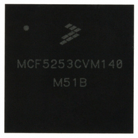
MCF5253CVM140 Freescale Semiconductor, MCF5253CVM140 Datasheet - Page 306

MCF5253CVM140
Manufacturer Part Number
MCF5253CVM140
Description
IC MPU 32BIT 140MHZ 225-MAPBGA
Manufacturer
Freescale Semiconductor
Series
MCF525xr
Datasheets
1.MCF5253VM140J.pdf
(34 pages)
2.MCF5253VM140J.pdf
(8 pages)
3.MCF5253VM140J.pdf
(648 pages)
4.MCF5253VM140J.pdf
(2 pages)
Specifications of MCF5253CVM140
Core Processor
Coldfire V2
Core Size
32-Bit
Speed
140MHz
Connectivity
CAN, EBI/EMI, I²C, QSPI, UART/USART, USB OTG
Peripherals
DMA, WDT
Program Memory Type
ROMless
Ram Size
128K x 8
Voltage - Supply (vcc/vdd)
1.08 V ~ 1.32 V
Data Converters
A/D 6x12b
Oscillator Type
External
Operating Temperature
-40°C ~ 85°C
Package / Case
225-MAPBGA
Family Name
MCF5xxx
Device Core
ColdFire V2
Device Core Size
32b
Frequency (max)
140MHz
Instruction Set Architecture
RISC
Supply Voltage 1 (typ)
1.2/3.3V
Operating Supply Voltage (max)
1.32/3.6V
Operating Supply Voltage (min)
1.08/3V
Operating Temp Range
-40C to 85C
Operating Temperature Classification
Industrial
Mounting
Surface Mount
Pin Count
225
Package Type
MA-BGA
Lead Free Status / RoHS Status
Lead free / RoHS Compliant
Number Of I /o
-
Eeprom Size
-
Program Memory Size
-
Lead Free Status / Rohs Status
Compliant
Available stocks
Company
Part Number
Manufacturer
Quantity
Price
Company:
Part Number:
MCF5253CVM140
Manufacturer:
FREESCALE
Quantity:
300
Company:
Part Number:
MCF5253CVM140
Manufacturer:
Freescale Semiconductor
Quantity:
10 000
Part Number:
MCF5253CVM140
Manufacturer:
FREESCALE
Quantity:
20 000
Company:
Part Number:
MCF5253CVM140J
Manufacturer:
Freescale Semiconductor
Quantity:
10 000
- MCF5253VM140J PDF datasheet
- MCF5253VM140J PDF datasheet #2
- MCF5253VM140J PDF datasheet #3
- MCF5253VM140J PDF datasheet #4
- Current page: 306 of 648
- Download datasheet (8Mb)
Address MBAR2 + 0x10 (reset 0x0fc8)
Audio Interface Module (AIM)
17.5
There are a total of three serial audio interfaces. Each interface can handle Philips I
protocol. Interface 1 is a receive/transmit interface. Interface 2 is transmit only, Interface 3 is a receive
only. Every serial audio interface block has a 32-bit configuration register associated with it.
Inversion of the LRCK clock only operates correctly on a slave receiver, therefore IIS3. If IIS1 is being
used for transmit and receive in master mode then LRCK will be inverted on both the input and the output.
Thereby cancelling the effect.
The SCLK and LRCK signals for each I
generated internally (outputs). See
Figure 17-2
description of the bit fields.
Figure 17-3
description of the bit fields.
17-8
Reset 0
Reset 0
W
W
R
R
31
15
Serial Audio Interface (I
CLOCKSEL
illustrates the valid bits in the IIS1 Configuration Registers and
illustrates the valid bits in the IIS2 Configuration Registers and
30
14
0
0
Each of the three I
or Sony EIAJ mode with either 32, 36, or 40 bits per word clock. Timing
diagrams describing each of these modes are given in the following
sections. The frequency of the clock and data signals is programmable, as is
the inversion of the bit clock (SCLK) or word clock (LRCK) for each I
interface.
29
13
0
0
28
12
0
0
CONTROL
TX FIFO
27
11
0
1
Figure 17-2. IIS1 Configuration Registers (0x10)
2
S interfaces is capable of operating in Philips I
Table
TXSOURCE
26
10
0
1
MCF5253 Reference Manual, Rev. 1
SELECT
25
2
0
1
9
S interface can either be inputs to the interface or they can be
17-5.
24
0
8
1
2
S/EIAJ) Register Descriptions
23
0
1
7
NOTE
SIZE
22
0
1
6
MODE
21
0
0
5
20
0
0
4
FREQUENCY
19
0
3
LRCK
1
EF/CFLG
INSERT
18
0
0
2
Table 17-5
Table 17-5
2
CFLG SAMPLE
LRCK INVERT
S mode
POSITION
2
Freescale Semiconductor
S or Sony EIAJ
Access: User read/write
2
17
0
0
S
1
provides the
provides the
TXSOURCE
SELECT
INVERT
SCLK
16
0
0
0
Related parts for MCF5253CVM140
Image
Part Number
Description
Manufacturer
Datasheet
Request
R
Part Number:
Description:
Mcf5253 Coldfire? Microprocessor Data Sheet
Manufacturer:
Freescale Semiconductor, Inc
Datasheet:
Part Number:
Description:
Manufacturer:
Freescale Semiconductor, Inc
Datasheet:
Part Number:
Description:
Manufacturer:
Freescale Semiconductor, Inc
Datasheet:
Part Number:
Description:
Manufacturer:
Freescale Semiconductor, Inc
Datasheet:
Part Number:
Description:
Manufacturer:
Freescale Semiconductor, Inc
Datasheet:
Part Number:
Description:
Manufacturer:
Freescale Semiconductor, Inc
Datasheet:
Part Number:
Description:
Manufacturer:
Freescale Semiconductor, Inc
Datasheet:
Part Number:
Description:
Manufacturer:
Freescale Semiconductor, Inc
Datasheet:
Part Number:
Description:
Manufacturer:
Freescale Semiconductor, Inc
Datasheet:
Part Number:
Description:
Manufacturer:
Freescale Semiconductor, Inc
Datasheet:
Part Number:
Description:
Manufacturer:
Freescale Semiconductor, Inc
Datasheet:
Part Number:
Description:
Manufacturer:
Freescale Semiconductor, Inc
Datasheet:
Part Number:
Description:
Manufacturer:
Freescale Semiconductor, Inc
Datasheet:
Part Number:
Description:
Manufacturer:
Freescale Semiconductor, Inc
Datasheet:
Part Number:
Description:
Manufacturer:
Freescale Semiconductor, Inc
Datasheet:


