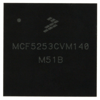
MCF5253CVM140 Freescale Semiconductor, MCF5253CVM140 Datasheet - Page 137

MCF5253CVM140
Manufacturer Part Number
MCF5253CVM140
Description
IC MPU 32BIT 140MHZ 225-MAPBGA
Manufacturer
Freescale Semiconductor
Series
MCF525xr
Datasheets
1.MCF5253VM140J.pdf
(34 pages)
2.MCF5253VM140J.pdf
(8 pages)
3.MCF5253VM140J.pdf
(648 pages)
4.MCF5253VM140J.pdf
(2 pages)
Specifications of MCF5253CVM140
Core Processor
Coldfire V2
Core Size
32-Bit
Speed
140MHz
Connectivity
CAN, EBI/EMI, I²C, QSPI, UART/USART, USB OTG
Peripherals
DMA, WDT
Program Memory Type
ROMless
Ram Size
128K x 8
Voltage - Supply (vcc/vdd)
1.08 V ~ 1.32 V
Data Converters
A/D 6x12b
Oscillator Type
External
Operating Temperature
-40°C ~ 85°C
Package / Case
225-MAPBGA
Family Name
MCF5xxx
Device Core
ColdFire V2
Device Core Size
32b
Frequency (max)
140MHz
Instruction Set Architecture
RISC
Supply Voltage 1 (typ)
1.2/3.3V
Operating Supply Voltage (max)
1.32/3.6V
Operating Supply Voltage (min)
1.08/3V
Operating Temp Range
-40C to 85C
Operating Temperature Classification
Industrial
Mounting
Surface Mount
Pin Count
225
Package Type
MA-BGA
Lead Free Status / RoHS Status
Lead free / RoHS Compliant
Number Of I /o
-
Eeprom Size
-
Program Memory Size
-
Lead Free Status / Rohs Status
Compliant
Available stocks
Company
Part Number
Manufacturer
Quantity
Price
Company:
Part Number:
MCF5253CVM140
Manufacturer:
FREESCALE
Quantity:
300
Company:
Part Number:
MCF5253CVM140
Manufacturer:
Freescale Semiconductor
Quantity:
10 000
Part Number:
MCF5253CVM140
Manufacturer:
FREESCALE
Quantity:
20 000
Company:
Part Number:
MCF5253CVM140J
Manufacturer:
Freescale Semiconductor
Quantity:
10 000
- MCF5253VM140J PDF datasheet
- MCF5253VM140J PDF datasheet #2
- MCF5253VM140J PDF datasheet #3
- MCF5253VM140J PDF datasheet #4
- Current page: 137 of 648
- Download datasheet (8Mb)
Figure 8-6
8.5.4
The MCF5253 can accommodate back-to-back bus cycles. The processor runs back-to-back bus cycles
whenever possible. For example, when a longword read is started on a word-size bus, and burst read enable
is disabled into the relevant chip select register, the processor will perform two word reads back to back.
Figure 8-7
Freescale Semiconductor
State Name
STATE 0
STATE 1
STATE 2
STATE 3
STATE 4
STATE 5
shows the description for the six states of a basic write cycle.
shows a read, followed by a write that occurs back to back.
Back-to-Back Bus Cycles
The write cycle is initiated in state 0 (S0). On the rising edge of BCLK, the MCF5253 places a valid address on
the address bus and drives RW low, if it is not already low.
The appropriate CS is asserted on the falling edge of BCLK.
The data bus is driven out of high impedance as data is placed on the bus on the rising edge of BCLK.
During state 3 (S3), the MCF5253 waits for a cycle termination signal (TA). If TA is not asserted before the rising
edge of BCLK at the end of the first clock cycle, the MCF5253 inserts wait states (full clock cycles) until TA is
asserted. TA is generated internally by the chip select module. If internal TA is requested (auto-acknowledge
enabled in the chip select control register, CSCR) then TA is generated internally by the chip select module.
During state 4, TA should be negated by the external device or if auto-acknowledge is enabled, negated internally
by the chip select module.
CS is negated on the falling edge of BCLK in state 5 (S5). The MCF5253 stops driving the address lines and RW,
terminating the write cycle. The data bus returns to high impedance on the rising edge of BCLK.
The rising edge of BCLK may be the start of state 0 for the next access cycle.
D[31:16]
A[23:1]
BCLK
CSx
RW
TA
Figure 8-6. Basic Write Bus Cycle
MCF5253 Reference Manual, Rev. 1
Table 8-7. Write Cycle States
S0
S1
Description
S2
Write
S3
S4
S5
Bus Operation
8-9
Related parts for MCF5253CVM140
Image
Part Number
Description
Manufacturer
Datasheet
Request
R
Part Number:
Description:
Mcf5253 Coldfire? Microprocessor Data Sheet
Manufacturer:
Freescale Semiconductor, Inc
Datasheet:
Part Number:
Description:
Manufacturer:
Freescale Semiconductor, Inc
Datasheet:
Part Number:
Description:
Manufacturer:
Freescale Semiconductor, Inc
Datasheet:
Part Number:
Description:
Manufacturer:
Freescale Semiconductor, Inc
Datasheet:
Part Number:
Description:
Manufacturer:
Freescale Semiconductor, Inc
Datasheet:
Part Number:
Description:
Manufacturer:
Freescale Semiconductor, Inc
Datasheet:
Part Number:
Description:
Manufacturer:
Freescale Semiconductor, Inc
Datasheet:
Part Number:
Description:
Manufacturer:
Freescale Semiconductor, Inc
Datasheet:
Part Number:
Description:
Manufacturer:
Freescale Semiconductor, Inc
Datasheet:
Part Number:
Description:
Manufacturer:
Freescale Semiconductor, Inc
Datasheet:
Part Number:
Description:
Manufacturer:
Freescale Semiconductor, Inc
Datasheet:
Part Number:
Description:
Manufacturer:
Freescale Semiconductor, Inc
Datasheet:
Part Number:
Description:
Manufacturer:
Freescale Semiconductor, Inc
Datasheet:
Part Number:
Description:
Manufacturer:
Freescale Semiconductor, Inc
Datasheet:
Part Number:
Description:
Manufacturer:
Freescale Semiconductor, Inc
Datasheet:


