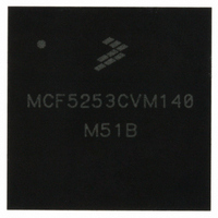
MCF5253CVM140 Freescale Semiconductor, MCF5253CVM140 Datasheet - Page 350

MCF5253CVM140
Manufacturer Part Number
MCF5253CVM140
Description
IC MPU 32BIT 140MHZ 225-MAPBGA
Manufacturer
Freescale Semiconductor
Series
MCF525xr
Datasheets
1.MCF5253VM140J.pdf
(34 pages)
2.MCF5253VM140J.pdf
(8 pages)
3.MCF5253VM140J.pdf
(648 pages)
4.MCF5253VM140J.pdf
(2 pages)
Specifications of MCF5253CVM140
Core Processor
Coldfire V2
Core Size
32-Bit
Speed
140MHz
Connectivity
CAN, EBI/EMI, I²C, QSPI, UART/USART, USB OTG
Peripherals
DMA, WDT
Program Memory Type
ROMless
Ram Size
128K x 8
Voltage - Supply (vcc/vdd)
1.08 V ~ 1.32 V
Data Converters
A/D 6x12b
Oscillator Type
External
Operating Temperature
-40°C ~ 85°C
Package / Case
225-MAPBGA
Family Name
MCF5xxx
Device Core
ColdFire V2
Device Core Size
32b
Frequency (max)
140MHz
Instruction Set Architecture
RISC
Supply Voltage 1 (typ)
1.2/3.3V
Operating Supply Voltage (max)
1.32/3.6V
Operating Supply Voltage (min)
1.08/3V
Operating Temp Range
-40C to 85C
Operating Temperature Classification
Industrial
Mounting
Surface Mount
Pin Count
225
Package Type
MA-BGA
Lead Free Status / RoHS Status
Lead free / RoHS Compliant
Number Of I /o
-
Eeprom Size
-
Program Memory Size
-
Lead Free Status / Rohs Status
Compliant
Available stocks
Company
Part Number
Manufacturer
Quantity
Price
Company:
Part Number:
MCF5253CVM140
Manufacturer:
FREESCALE
Quantity:
300
Company:
Part Number:
MCF5253CVM140
Manufacturer:
Freescale Semiconductor
Quantity:
10 000
Part Number:
MCF5253CVM140
Manufacturer:
FREESCALE
Quantity:
20 000
Company:
Part Number:
MCF5253CVM140J
Manufacturer:
Freescale Semiconductor
Quantity:
10 000
- MCF5253VM140J PDF datasheet
- MCF5253VM140J PDF datasheet #2
- MCF5253VM140J PDF datasheet #3
- MCF5253VM140J PDF datasheet #4
- Current page: 350 of 648
- Download datasheet (8Mb)
I
another device clock is still within its low period. Therefore, SCL is held low by the device with the longest
low period. Devices with shorter low periods enter a high wait state during this time (see
When all devices concerned have counted off their low period, the SCL line is released and pulled high.
At this point, there is no difference between the device clocks and the state of the SCL line and all the
devices start counting their high periods. The first device to complete its high period pulls the SCL line
low again.
18.4.8
The clock synchronization mechanism can be used as a handshake in data transfer. Slave devices can hold
the SCL line low after completion of one byte transfer (9 clocks). In such cases, it halts the bus clock and
forces the master clock into wait states until the slave releases the SCL line.
18.4.9
Slaves can use the clock synchronization mechanism to slow down the transfer bit rate. After the master
has driven SCL low, the slave can drive SCL low for the required period and then release it. If the slave
SCL low period is greater than the master SCL low period, the resulting SCL bus signal low period is
stretched.
18.5
Internal configuration of the five registers used in the I
Table 18-1
18-6
2
C Modules
I
2
shows the register summary of the I
SCL1
SCL2
Handshaking
Clock Stretching
C Memory Map and Register Descriptions
SCL
INTERNAL COUNTER RESET
MBAR+$280
MBAR+$284
Address
Table 18-1. I
Figure 18-3. Synchronized Clock SCL
MCF5253 Reference Manual, Rev. 1
2
C Interfaces Register Summary
I
2
C Frequency Divider Register (MFDR)
2
I
C interface.
2
C Address Register (MADR)
I
2
WAIT
C Module Registers
2
C interface are detailed in the following sections.
START COUNTING HIGH PERIOD
Freescale Semiconductor
Figure
18-3).
Related parts for MCF5253CVM140
Image
Part Number
Description
Manufacturer
Datasheet
Request
R
Part Number:
Description:
Mcf5253 Coldfire? Microprocessor Data Sheet
Manufacturer:
Freescale Semiconductor, Inc
Datasheet:
Part Number:
Description:
Manufacturer:
Freescale Semiconductor, Inc
Datasheet:
Part Number:
Description:
Manufacturer:
Freescale Semiconductor, Inc
Datasheet:
Part Number:
Description:
Manufacturer:
Freescale Semiconductor, Inc
Datasheet:
Part Number:
Description:
Manufacturer:
Freescale Semiconductor, Inc
Datasheet:
Part Number:
Description:
Manufacturer:
Freescale Semiconductor, Inc
Datasheet:
Part Number:
Description:
Manufacturer:
Freescale Semiconductor, Inc
Datasheet:
Part Number:
Description:
Manufacturer:
Freescale Semiconductor, Inc
Datasheet:
Part Number:
Description:
Manufacturer:
Freescale Semiconductor, Inc
Datasheet:
Part Number:
Description:
Manufacturer:
Freescale Semiconductor, Inc
Datasheet:
Part Number:
Description:
Manufacturer:
Freescale Semiconductor, Inc
Datasheet:
Part Number:
Description:
Manufacturer:
Freescale Semiconductor, Inc
Datasheet:
Part Number:
Description:
Manufacturer:
Freescale Semiconductor, Inc
Datasheet:
Part Number:
Description:
Manufacturer:
Freescale Semiconductor, Inc
Datasheet:
Part Number:
Description:
Manufacturer:
Freescale Semiconductor, Inc
Datasheet:


