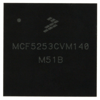
MCF5253CVM140 Freescale Semiconductor, MCF5253CVM140 Datasheet - Page 243

MCF5253CVM140
Manufacturer Part Number
MCF5253CVM140
Description
IC MPU 32BIT 140MHZ 225-MAPBGA
Manufacturer
Freescale Semiconductor
Series
MCF525xr
Datasheets
1.MCF5253VM140J.pdf
(34 pages)
2.MCF5253VM140J.pdf
(8 pages)
3.MCF5253VM140J.pdf
(648 pages)
4.MCF5253VM140J.pdf
(2 pages)
Specifications of MCF5253CVM140
Core Processor
Coldfire V2
Core Size
32-Bit
Speed
140MHz
Connectivity
CAN, EBI/EMI, I²C, QSPI, UART/USART, USB OTG
Peripherals
DMA, WDT
Program Memory Type
ROMless
Ram Size
128K x 8
Voltage - Supply (vcc/vdd)
1.08 V ~ 1.32 V
Data Converters
A/D 6x12b
Oscillator Type
External
Operating Temperature
-40°C ~ 85°C
Package / Case
225-MAPBGA
Family Name
MCF5xxx
Device Core
ColdFire V2
Device Core Size
32b
Frequency (max)
140MHz
Instruction Set Architecture
RISC
Supply Voltage 1 (typ)
1.2/3.3V
Operating Supply Voltage (max)
1.32/3.6V
Operating Supply Voltage (min)
1.08/3V
Operating Temp Range
-40C to 85C
Operating Temperature Classification
Industrial
Mounting
Surface Mount
Pin Count
225
Package Type
MA-BGA
Lead Free Status / RoHS Status
Lead free / RoHS Compliant
Number Of I /o
-
Eeprom Size
-
Program Memory Size
-
Lead Free Status / Rohs Status
Compliant
Available stocks
Company
Part Number
Manufacturer
Quantity
Price
Company:
Part Number:
MCF5253CVM140
Manufacturer:
FREESCALE
Quantity:
300
Company:
Part Number:
MCF5253CVM140
Manufacturer:
Freescale Semiconductor
Quantity:
10 000
Part Number:
MCF5253CVM140
Manufacturer:
FREESCALE
Quantity:
20 000
Company:
Part Number:
MCF5253CVM140J
Manufacturer:
Freescale Semiconductor
Quantity:
10 000
- MCF5253VM140J PDF datasheet
- MCF5253VM140J PDF datasheet #2
- MCF5253VM140J PDF datasheet #3
- MCF5253VM140J PDF datasheet #4
- Current page: 243 of 648
- Download datasheet (8Mb)
14.7.1.1
The four DMA channels are prioritized in ascending order (channel 0 having highest priority and channel
3 having the lowest) or as determined by the BWC bits in the DCR. If the BWC bits for a DMA channel
are set to 000, then that channel has priority over the channel immediately preceding it. For example, if
DMA channel 3 has the BWC bits set to 000, it has priority over DMA channel 2 but not over DMA
channel 1. This is assuming that DMA channel 2 has something other than all zeroes in the BWC bits.
Another example would be the case where the BWC bits in only DMA 2 and DMA 1 are all zeroes. In this
case, DMA 1 would have priority over DMA 0 and DMA 2. The BWC bits being zero in DMA 2 in this
case have no effect on prioritization.
In the case of simultaneous external requests, the prioritization is either ascending or as determined by each
channels BWC bits as described in the previous paragraphs.
14.7.1.2
The following are some general comments on programming the DMA:
The SAR is loaded with the source (read) address. If the transfer is from a peripheral device to memory,
the source address is the location of the peripheral data register. If the transfer is from memory to a
peripheral device or memory to memory, the source address is the starting address of the data block. This
address can be any byte address.
The DAR should contain the destination (write) address. If the transfer is from a peripheral device to
memory, or memory to memory, the DAR is loaded with the starting address of the data block to be written.
If the transfer is from memory to a peripheral device, the DAR is loaded with the address of the peripheral
data register. This address can be any byte address.
The manner in which the SAR and DAR change after each cycle depends on the values in the DCR SSIZE
and DSIZE fields and the SINC and DINC bits, and the starting address in the SAR and DAR. If
programmed to increment, the increment value is 1, 2, 4, or 16 for byte, word, longword, or line operands,
respectively. If the address register is programmed to remain unchanged (no count), the register is not
incremented after the operand transfer.
The BCR must be loaded with the number of byte transfers that are to occur. This register is decremented
by 1, 2, 4, or 16 at the end of each transfer. The DSR must be cleared for channel startup.
Once the channel has been initialized, it is started by writing a one to the START bit in the DCR or
asserting the REQUEST signal, depending on the status of the EEXT bit in the DCR. Programming the
channel for processor request causes the channel to request the bus and start transferring data immediately.
If the channel is programmed for periphery request, REQUEST must be asserted before the channel
requests the bus.
If any fields in the DCR are modified while the channel is active, that change is effective immediately. To
avoid any problems with changing the setup for the DMA channel, a 1 should be written to the DONE bit
in the DSR to stop the DMA channel.
Freescale Semiconductor
•
•
No mechanism exists for preventing writes to control registers during DMA accesses
If the BWC of sequential channels are equivalent, channel priority is in ascending order
Channel Prioritization
Programming the DMA
MCF5253 Reference Manual, Rev. 1
DMA Controller
14-15
Related parts for MCF5253CVM140
Image
Part Number
Description
Manufacturer
Datasheet
Request
R
Part Number:
Description:
Mcf5253 Coldfire? Microprocessor Data Sheet
Manufacturer:
Freescale Semiconductor, Inc
Datasheet:
Part Number:
Description:
Manufacturer:
Freescale Semiconductor, Inc
Datasheet:
Part Number:
Description:
Manufacturer:
Freescale Semiconductor, Inc
Datasheet:
Part Number:
Description:
Manufacturer:
Freescale Semiconductor, Inc
Datasheet:
Part Number:
Description:
Manufacturer:
Freescale Semiconductor, Inc
Datasheet:
Part Number:
Description:
Manufacturer:
Freescale Semiconductor, Inc
Datasheet:
Part Number:
Description:
Manufacturer:
Freescale Semiconductor, Inc
Datasheet:
Part Number:
Description:
Manufacturer:
Freescale Semiconductor, Inc
Datasheet:
Part Number:
Description:
Manufacturer:
Freescale Semiconductor, Inc
Datasheet:
Part Number:
Description:
Manufacturer:
Freescale Semiconductor, Inc
Datasheet:
Part Number:
Description:
Manufacturer:
Freescale Semiconductor, Inc
Datasheet:
Part Number:
Description:
Manufacturer:
Freescale Semiconductor, Inc
Datasheet:
Part Number:
Description:
Manufacturer:
Freescale Semiconductor, Inc
Datasheet:
Part Number:
Description:
Manufacturer:
Freescale Semiconductor, Inc
Datasheet:
Part Number:
Description:
Manufacturer:
Freescale Semiconductor, Inc
Datasheet:


