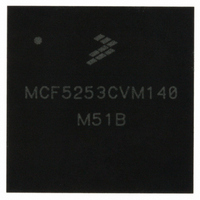
MCF5253CVM140 Freescale Semiconductor, MCF5253CVM140 Datasheet - Page 326

MCF5253CVM140
Manufacturer Part Number
MCF5253CVM140
Description
IC MPU 32BIT 140MHZ 225-MAPBGA
Manufacturer
Freescale Semiconductor
Series
MCF525xr
Datasheets
1.MCF5253VM140J.pdf
(34 pages)
2.MCF5253VM140J.pdf
(8 pages)
3.MCF5253VM140J.pdf
(648 pages)
4.MCF5253VM140J.pdf
(2 pages)
Specifications of MCF5253CVM140
Core Processor
Coldfire V2
Core Size
32-Bit
Speed
140MHz
Connectivity
CAN, EBI/EMI, I²C, QSPI, UART/USART, USB OTG
Peripherals
DMA, WDT
Program Memory Type
ROMless
Ram Size
128K x 8
Voltage - Supply (vcc/vdd)
1.08 V ~ 1.32 V
Data Converters
A/D 6x12b
Oscillator Type
External
Operating Temperature
-40°C ~ 85°C
Package / Case
225-MAPBGA
Family Name
MCF5xxx
Device Core
ColdFire V2
Device Core Size
32b
Frequency (max)
140MHz
Instruction Set Architecture
RISC
Supply Voltage 1 (typ)
1.2/3.3V
Operating Supply Voltage (max)
1.32/3.6V
Operating Supply Voltage (min)
1.08/3V
Operating Temp Range
-40C to 85C
Operating Temperature Classification
Industrial
Mounting
Surface Mount
Pin Count
225
Package Type
MA-BGA
Lead Free Status / RoHS Status
Lead free / RoHS Compliant
Number Of I /o
-
Eeprom Size
-
Program Memory Size
-
Lead Free Status / Rohs Status
Compliant
Available stocks
Company
Part Number
Manufacturer
Quantity
Price
Company:
Part Number:
MCF5253CVM140
Manufacturer:
FREESCALE
Quantity:
300
Company:
Part Number:
MCF5253CVM140
Manufacturer:
Freescale Semiconductor
Quantity:
10 000
Part Number:
MCF5253CVM140
Manufacturer:
FREESCALE
Quantity:
20 000
Company:
Part Number:
MCF5253CVM140J
Manufacturer:
Freescale Semiconductor
Quantity:
10 000
- MCF5253VM140J PDF datasheet
- MCF5253VM140J PDF datasheet #2
- MCF5253VM140J PDF datasheet #3
- MCF5253VM140J PDF datasheet #4
- Current page: 326 of 648
- Download datasheet (8Mb)
1
2
Audio Interface Module (AIM)
17.7.2
17-28
MBAR2 +
Address
Multiple addresses for PDOR/PDIR fields are intended for easy use of MOVEM instruction to move data into and out of the FIFOs.
The data read at each address of any range is exactly the same, being the next sample in/out of the FIFO. There is no difference
in FIFO operation between a read at address e.g. 0x74, 0x78, 0x7C.
There are memory overlaps between PDIR’s and PDOR’s. PDOR’s cannot be read, PDIR cannot be written.
0x3C
0x4C
0x5C
0x6C
0x7C
0x7C
0x34
0x38
0x40
0x44
0x48
0x50
0x54
0x58
0x60
0x64
0x68
0x70
0x74
0x78
0x80
0x74
0x78
0x80
•
•
•
•
PDOR1-L, PDOR1-R: (Processor Data Out 1). These are 32-bit registers. Both registers have 4
consecutive longword addresses assigned (multiple decode). This allows easy transfer of multiple
samples using MOVEM instructions. Data written to these registers will end in one of the FIFO ‘s
(Figure
PDOR2-L, PDOR2-R: (Processor Data Out 2). Same function as PDOR1. Both (PDOR2-L and
PDOR2-R) registers occupy 4 consecutive longword addresses (multiple decoded.) Data written to
it will end in one of the FIFO ‘s. (fig. 17-1) 12,14,17, 17a, 17b or 25.
PDOR3: (Processor Data Out3). Same function as PDOR1. But it is a single 32-bit register which
contains both Left + Right data in 16-bit precision occupying 4 consecutive longword addresses.
Data written to it will end in one of the FIFO ‘s. (fig 17-1) 12,14, 17a, 17b or 25.
PDIR1-L, PDIR1-R (Processor data in). Used to transfer data to the processor. These 32-bit
registers, each occupy 4 consecutive longword addresses are used to read data from the audio bus.
PDOR1-R
PDOR2-R
PDOR1-L
PDOR2-L
PDOR3
PDIR2
Data Exchange Register Overview
Name
17-1) 12, 14, 17, 17a, 17b or 25. The format of data in the registers is defined below.
Width
Table 17-14. Data Exchange Register Descriptions (continued)
32
32
32
32
32
32
Processor data out 1 Left.
Multiple address to write this register allows MOVEM instruction to write FIFO.
Processor data out 1 Right
Multiple address to write this register allows MOVEM instruction to write FIFO
Processor data out 2 Left
Multiple address to write this register allows MOVEM instruction to write FIFO
Processor data out 2 Right
Multiple address to write this register allows MOVEM instruction to write FIFO
Processor data out 3 left + right
Processor data in 3 left + right
MCF5253 Reference Manual, Rev. 1
Description
1, 2
Freescale Semiconductor
Reset
Value
undef
undef
undef
undef
undef
undef
Access
W
W
W
W
W
R
Related parts for MCF5253CVM140
Image
Part Number
Description
Manufacturer
Datasheet
Request
R
Part Number:
Description:
Mcf5253 Coldfire? Microprocessor Data Sheet
Manufacturer:
Freescale Semiconductor, Inc
Datasheet:
Part Number:
Description:
Manufacturer:
Freescale Semiconductor, Inc
Datasheet:
Part Number:
Description:
Manufacturer:
Freescale Semiconductor, Inc
Datasheet:
Part Number:
Description:
Manufacturer:
Freescale Semiconductor, Inc
Datasheet:
Part Number:
Description:
Manufacturer:
Freescale Semiconductor, Inc
Datasheet:
Part Number:
Description:
Manufacturer:
Freescale Semiconductor, Inc
Datasheet:
Part Number:
Description:
Manufacturer:
Freescale Semiconductor, Inc
Datasheet:
Part Number:
Description:
Manufacturer:
Freescale Semiconductor, Inc
Datasheet:
Part Number:
Description:
Manufacturer:
Freescale Semiconductor, Inc
Datasheet:
Part Number:
Description:
Manufacturer:
Freescale Semiconductor, Inc
Datasheet:
Part Number:
Description:
Manufacturer:
Freescale Semiconductor, Inc
Datasheet:
Part Number:
Description:
Manufacturer:
Freescale Semiconductor, Inc
Datasheet:
Part Number:
Description:
Manufacturer:
Freescale Semiconductor, Inc
Datasheet:
Part Number:
Description:
Manufacturer:
Freescale Semiconductor, Inc
Datasheet:
Part Number:
Description:
Manufacturer:
Freescale Semiconductor, Inc
Datasheet:


