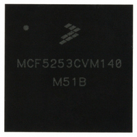
MCF5253CVM140 Freescale Semiconductor, MCF5253CVM140 Datasheet - Page 432

MCF5253CVM140
Manufacturer Part Number
MCF5253CVM140
Description
IC MPU 32BIT 140MHZ 225-MAPBGA
Manufacturer
Freescale Semiconductor
Series
MCF525xr
Datasheets
1.MCF5253VM140J.pdf
(34 pages)
2.MCF5253VM140J.pdf
(8 pages)
3.MCF5253VM140J.pdf
(648 pages)
4.MCF5253VM140J.pdf
(2 pages)
Specifications of MCF5253CVM140
Core Processor
Coldfire V2
Core Size
32-Bit
Speed
140MHz
Connectivity
CAN, EBI/EMI, I²C, QSPI, UART/USART, USB OTG
Peripherals
DMA, WDT
Program Memory Type
ROMless
Ram Size
128K x 8
Voltage - Supply (vcc/vdd)
1.08 V ~ 1.32 V
Data Converters
A/D 6x12b
Oscillator Type
External
Operating Temperature
-40°C ~ 85°C
Package / Case
225-MAPBGA
Family Name
MCF5xxx
Device Core
ColdFire V2
Device Core Size
32b
Frequency (max)
140MHz
Instruction Set Architecture
RISC
Supply Voltage 1 (typ)
1.2/3.3V
Operating Supply Voltage (max)
1.32/3.6V
Operating Supply Voltage (min)
1.08/3V
Operating Temp Range
-40C to 85C
Operating Temperature Classification
Industrial
Mounting
Surface Mount
Pin Count
225
Package Type
MA-BGA
Lead Free Status / RoHS Status
Lead free / RoHS Compliant
Number Of I /o
-
Eeprom Size
-
Program Memory Size
-
Lead Free Status / Rohs Status
Compliant
Available stocks
Company
Part Number
Manufacturer
Quantity
Price
Company:
Part Number:
MCF5253CVM140
Manufacturer:
FREESCALE
Quantity:
300
Company:
Part Number:
MCF5253CVM140
Manufacturer:
Freescale Semiconductor
Quantity:
10 000
Part Number:
MCF5253CVM140
Manufacturer:
FREESCALE
Quantity:
20 000
Company:
Part Number:
MCF5253CVM140J
Manufacturer:
Freescale Semiconductor
Quantity:
10 000
- MCF5253VM140J PDF datasheet
- MCF5253VM140J PDF datasheet #2
- MCF5253VM140J PDF datasheet #3
- MCF5253VM140J PDF datasheet #4
- Current page: 432 of 648
- Download datasheet (8Mb)
Advanced Technology Attachment Controller (ATA)
This electrical spec must be met for the pads used on the ATA I/Os if no bus buffers and bus transceivers
are used.
Alternative is to use bus buffers. This is the only way to operate the ATA interface if 3.3 V or 5.0 V
compatibility on the ATA bus is wanted, and no 3.3 V or 5.0 V tolerant pads on the device are available.
The use of bus buffers introduces delay on the bus and introduces skew between signal lines. These factors
will make it difficult to operate the bus at the highest speed (UDMA-5) when bus buffers are used. If fast
UDMA mode operation is needed, this may not be compatible with bus buffers.
Another area of attention is the slew rate limit imposed by the ATA specification on the ATA bus.
According to this limit, any signal driven on the bus should have a slew rate between 0.4 and 1.2 V/ns with
a 40 pF load. Not many vendors of bus buffers specify slew rate of the outgoing signals.
23.4.3
Timing on the ATA bus is explained in this section. It is also explained how to make sure the ATA interface
meets timing. Timing is explained with timing figures and also equations are provided that need to be
fulfilled for the host to meet timing.
23.4.3.1
In the timing equations, some timing parameters are used. These parameters depend on the implementation
of the ATA interface on silicon, the bus buffer used, the cable delay and cable skew. Refer to
for the list of parameters used to specify the ATA timing.
23-6
T
ti_ds
ti_dh
tco
tsu
tsui
thi
tskew1 Max difference in propagation delay bus clock L-to-H to any of following signals:
tskew2 Max difference in buffer propagation delay for any of following signals:
tskew3 Max difference in buffer propagation delay for any of following signals:
tbuf
tcable1 Cable propagation delay for ATA_Dx
tcable2 Cable propagation delay for control signals:
Name
Bus clock period
Set-up time ATA_Dx to ATA_IORDY edge (UDMA-in only)
hold time ATA_IORDY edge to ATA_Dx (UDMA-in only)
Propagation delay bus clock L-to-H to the following signals:
ATA_CS0, ATA_CS1. ATA_CS2. ATA_A2. ATA_A1, ATA_A0, ATA_DIOR, ATA_DIOW,
ATA_DMACK, ATA_Dx
Setup time ATA_Dx to bus clock L-to-H
Setup time ATA_IORDY to bus clock H-to-L
Hold time ATA_IORDY to bus clock H to L
ATA_CS0, ATA_CS1. ATA_CS2. ATA_A2. ATA_A1, ATA_A0, ATA_DIOR, ATA_DIOW,
ATA_DMACK, ATA_Dx (write)
Max buffer propagation delay
ATA_CS0, ATA_CS1. ATA_CS2. ATA_A2. ATA_A1, ATA_A0, ATA_DIOR, ATA_DIOW,
ATA_DMACK, ATA_Dx (write)
ATA_IORDY, ATA_Dx (read)
ATA_DIOR, ATA_DIOW, ATA_IORDY, ATA_DMACK
Timing on ATA Bus
Timing Parameters
MCF5253 Reference Manual, Rev. 1
Table 23-2. Timing Parameters
Meaning
Freescale Semiconductor
top level design
top level design
top level design
top level design
top level design
top level design
top level design
clock generator
Controlled by
transceiver
transceiver
transceiver
cable
cable
Table 23-2
Related parts for MCF5253CVM140
Image
Part Number
Description
Manufacturer
Datasheet
Request
R
Part Number:
Description:
Mcf5253 Coldfire? Microprocessor Data Sheet
Manufacturer:
Freescale Semiconductor, Inc
Datasheet:
Part Number:
Description:
Manufacturer:
Freescale Semiconductor, Inc
Datasheet:
Part Number:
Description:
Manufacturer:
Freescale Semiconductor, Inc
Datasheet:
Part Number:
Description:
Manufacturer:
Freescale Semiconductor, Inc
Datasheet:
Part Number:
Description:
Manufacturer:
Freescale Semiconductor, Inc
Datasheet:
Part Number:
Description:
Manufacturer:
Freescale Semiconductor, Inc
Datasheet:
Part Number:
Description:
Manufacturer:
Freescale Semiconductor, Inc
Datasheet:
Part Number:
Description:
Manufacturer:
Freescale Semiconductor, Inc
Datasheet:
Part Number:
Description:
Manufacturer:
Freescale Semiconductor, Inc
Datasheet:
Part Number:
Description:
Manufacturer:
Freescale Semiconductor, Inc
Datasheet:
Part Number:
Description:
Manufacturer:
Freescale Semiconductor, Inc
Datasheet:
Part Number:
Description:
Manufacturer:
Freescale Semiconductor, Inc
Datasheet:
Part Number:
Description:
Manufacturer:
Freescale Semiconductor, Inc
Datasheet:
Part Number:
Description:
Manufacturer:
Freescale Semiconductor, Inc
Datasheet:
Part Number:
Description:
Manufacturer:
Freescale Semiconductor, Inc
Datasheet:


