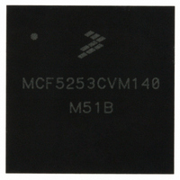
MCF5253CVM140 Freescale Semiconductor, MCF5253CVM140 Datasheet - Page 242

MCF5253CVM140
Manufacturer Part Number
MCF5253CVM140
Description
IC MPU 32BIT 140MHZ 225-MAPBGA
Manufacturer
Freescale Semiconductor
Series
MCF525xr
Datasheets
1.MCF5253VM140J.pdf
(34 pages)
2.MCF5253VM140J.pdf
(8 pages)
3.MCF5253VM140J.pdf
(648 pages)
4.MCF5253VM140J.pdf
(2 pages)
Specifications of MCF5253CVM140
Core Processor
Coldfire V2
Core Size
32-Bit
Speed
140MHz
Connectivity
CAN, EBI/EMI, I²C, QSPI, UART/USART, USB OTG
Peripherals
DMA, WDT
Program Memory Type
ROMless
Ram Size
128K x 8
Voltage - Supply (vcc/vdd)
1.08 V ~ 1.32 V
Data Converters
A/D 6x12b
Oscillator Type
External
Operating Temperature
-40°C ~ 85°C
Package / Case
225-MAPBGA
Family Name
MCF5xxx
Device Core
ColdFire V2
Device Core Size
32b
Frequency (max)
140MHz
Instruction Set Architecture
RISC
Supply Voltage 1 (typ)
1.2/3.3V
Operating Supply Voltage (max)
1.32/3.6V
Operating Supply Voltage (min)
1.08/3V
Operating Temp Range
-40C to 85C
Operating Temperature Classification
Industrial
Mounting
Surface Mount
Pin Count
225
Package Type
MA-BGA
Lead Free Status / RoHS Status
Lead free / RoHS Compliant
Number Of I /o
-
Eeprom Size
-
Program Memory Size
-
Lead Free Status / Rohs Status
Compliant
Available stocks
Company
Part Number
Manufacturer
Quantity
Price
Company:
Part Number:
MCF5253CVM140
Manufacturer:
FREESCALE
Quantity:
300
Company:
Part Number:
MCF5253CVM140
Manufacturer:
Freescale Semiconductor
Quantity:
10 000
Part Number:
MCF5253CVM140
Manufacturer:
FREESCALE
Quantity:
20 000
Company:
Part Number:
MCF5253CVM140J
Manufacturer:
Freescale Semiconductor
Quantity:
10 000
- MCF5253VM140J PDF datasheet
- MCF5253VM140J PDF datasheet #2
- MCF5253VM140J PDF datasheet #3
- MCF5253VM140J PDF datasheet #4
- Current page: 242 of 648
- Download datasheet (8Mb)
DMA Controller
In the event of a termination error, the BES (DSR[5]) and DONE bit (DSR[0]) are set and no further DMA
transactions take place.
14.6.1.2
The DMA controller module drives the value in the destination address register (DAR) onto the address
bus. If the DINC bit (DCR[19]) is set, then the DAR increments by the appropriate number of bytes at the
completion of a successful write cycle. The byte count register (BCR) decrements by the appropriate
number of bytes. The DONE bit (DSR[0]) is set when the BCR reaches zero. If the BCR is greater than
zero, then another read/write transfer is initiated. If the byte count register (BCR) is a multiple of the
programmed bandwidth control (BWC), then the DMA request signal is negated until termination of the
bus cycle to allow the internal arbiter to switch masters.
In the event of a termination error, the BES (DSR[5]) and DONE bit (DSR[0]) are set and no further DMA
transactions takes place.
14.7
In the following section, the term DMA request implies that the START bit (DCR[16]) is set or the EEXT
bit (DCR[30]) is set, followed by assertion of REQUEST. The START bit is cleared when the channel
begins an internal access.
Before initiating a transfer, the DMA controller module verifies that the source size (SSIZE = DSC[21:20])
and destination size (DSIZE = DSR[18:17]) for dual-address access are consistent with the source address
and destination address. The CE bit is also set if inconsistency is found between the destination size and
the source size in the BCR for dual-address access. If a misalignment is detected, no transfer occurs and
the configuration error bit (CE = DSR[6]) is set. Depending on the configuration of the DCR, an interrupt
event may be issued when the CE bit is set.
A read/write transfer refers to a dual-address access in which a number of bytes are read from the source
address and written to the destination address. The number of bytes in the transfer is determined by the
larger of the sizes specified by the source and destination size encoding. See
The source and destination address registers (SAR and DAR) increment at the completion of a successful
address phase. The BCR decrements at the completion of a successful address write phase. A successful
address phase occurs when a valid address request is not held by the arbiter.
14.7.1
Before starting a block transfer operation, the channel registers must be initialized with information
describing the channel configuration, request-generation method, and data block. This initialization is
accomplished by programming the appropriate information into the channel registers.
14-14
DMA Transfer Functional Description
Channel Initialization and Startup
Dual-Address Write
If the auto-align bit (AA = DCR[28]) is set, error checking is performed on
the appropriate registers only.
MCF5253 Reference Manual, Rev. 1
NOTE
Table 14-10
Freescale Semiconductor
and
Table
14-11.
Related parts for MCF5253CVM140
Image
Part Number
Description
Manufacturer
Datasheet
Request
R
Part Number:
Description:
Mcf5253 Coldfire? Microprocessor Data Sheet
Manufacturer:
Freescale Semiconductor, Inc
Datasheet:
Part Number:
Description:
Manufacturer:
Freescale Semiconductor, Inc
Datasheet:
Part Number:
Description:
Manufacturer:
Freescale Semiconductor, Inc
Datasheet:
Part Number:
Description:
Manufacturer:
Freescale Semiconductor, Inc
Datasheet:
Part Number:
Description:
Manufacturer:
Freescale Semiconductor, Inc
Datasheet:
Part Number:
Description:
Manufacturer:
Freescale Semiconductor, Inc
Datasheet:
Part Number:
Description:
Manufacturer:
Freescale Semiconductor, Inc
Datasheet:
Part Number:
Description:
Manufacturer:
Freescale Semiconductor, Inc
Datasheet:
Part Number:
Description:
Manufacturer:
Freescale Semiconductor, Inc
Datasheet:
Part Number:
Description:
Manufacturer:
Freescale Semiconductor, Inc
Datasheet:
Part Number:
Description:
Manufacturer:
Freescale Semiconductor, Inc
Datasheet:
Part Number:
Description:
Manufacturer:
Freescale Semiconductor, Inc
Datasheet:
Part Number:
Description:
Manufacturer:
Freescale Semiconductor, Inc
Datasheet:
Part Number:
Description:
Manufacturer:
Freescale Semiconductor, Inc
Datasheet:
Part Number:
Description:
Manufacturer:
Freescale Semiconductor, Inc
Datasheet:


