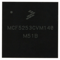
MCF5253CVM140 Freescale Semiconductor, MCF5253CVM140 Datasheet - Page 112

MCF5253CVM140
Manufacturer Part Number
MCF5253CVM140
Description
IC MPU 32BIT 140MHZ 225-MAPBGA
Manufacturer
Freescale Semiconductor
Series
MCF525xr
Datasheets
1.MCF5253VM140J.pdf
(34 pages)
2.MCF5253VM140J.pdf
(8 pages)
3.MCF5253VM140J.pdf
(648 pages)
4.MCF5253VM140J.pdf
(2 pages)
Specifications of MCF5253CVM140
Core Processor
Coldfire V2
Core Size
32-Bit
Speed
140MHz
Connectivity
CAN, EBI/EMI, I²C, QSPI, UART/USART, USB OTG
Peripherals
DMA, WDT
Program Memory Type
ROMless
Ram Size
128K x 8
Voltage - Supply (vcc/vdd)
1.08 V ~ 1.32 V
Data Converters
A/D 6x12b
Oscillator Type
External
Operating Temperature
-40°C ~ 85°C
Package / Case
225-MAPBGA
Family Name
MCF5xxx
Device Core
ColdFire V2
Device Core Size
32b
Frequency (max)
140MHz
Instruction Set Architecture
RISC
Supply Voltage 1 (typ)
1.2/3.3V
Operating Supply Voltage (max)
1.32/3.6V
Operating Supply Voltage (min)
1.08/3V
Operating Temp Range
-40C to 85C
Operating Temperature Classification
Industrial
Mounting
Surface Mount
Pin Count
225
Package Type
MA-BGA
Lead Free Status / RoHS Status
Lead free / RoHS Compliant
Number Of I /o
-
Eeprom Size
-
Program Memory Size
-
Lead Free Status / Rohs Status
Compliant
Available stocks
Company
Part Number
Manufacturer
Quantity
Price
Company:
Part Number:
MCF5253CVM140
Manufacturer:
FREESCALE
Quantity:
300
Company:
Part Number:
MCF5253CVM140
Manufacturer:
Freescale Semiconductor
Quantity:
10 000
Part Number:
MCF5253CVM140
Manufacturer:
FREESCALE
Quantity:
20 000
Company:
Part Number:
MCF5253CVM140J
Manufacturer:
Freescale Semiconductor
Quantity:
10 000
- MCF5253VM140J PDF datasheet
- MCF5253VM140J PDF datasheet #2
- MCF5253VM140J PDF datasheet #3
- MCF5253VM140J PDF datasheet #4
- Current page: 112 of 648
- Download datasheet (8Mb)
Synchronous DRAM Controller Module
7.4
To reduce system logic and to support a variety of SDRAM sizes, the DRAM controller provides SDRAM
control signals as well as a multiplexed row address and column address to the SDRAM.
When SDRAM blocks are accessed, the DRAM controller can operate in either burst or continuous page
mode. The following sections describe the DRAM controller interface to SDRAM, the supported bus
transfers, and initialization.
7.4.1
Table
to determine the correct address line connections for interfacing the MCF5253 to SDRAM. Note: that there
are separate connection tables for 4Mb to 128 Mb devices and 256 Mb devices.
Specifically for the 256Mb devices the tables change due to the fact that we need to have a A24 address
line. But with the MCF5253 A24 and A20 are shared on the same pin. This means that when we program
the A20/A24 pin to be A24. We no longer have A20 available to any memory device connected to the
memory bus.
To use the tables, find the one that corresponds to the number of column address lines on the SDRAM.
Most SDRAMs likely have fewer address lines than are shown in the tables, so follow only the connections
shown until all SDRAM address lines are connected.
7-8
AMx
Bits
6–1
7
0
V
7-7,
Reserved, should be cleared.
Address modifier masks. Determine which accesses can occur in a given DRAM block.
0 Allow access type to hit in DRAM
1 Do not allow access type to hit in DRAM
Valid. Cleared at reset to ensure that the DRAM block is not erroneously decoded.
0 Do not decode DRAM accesses.
1 Registers controlling the DRAM block are initialized; DRAM accesses can be decoded.
General Synchronous Operation Guidelines
Table
Address Multiplexing
Table 7-6. DRAM Controller Mask Register (DMR0) Field Descriptions (continued)
7-8,
AM
SC
SD
UC
UD
Bit
C/I
Table
CPU space/interrupt
acknowledge
Alternate master
Supervisor code
Supervisor data
User code
User data
7-9,
Associated Access Type
Table
MCF5253 Reference Manual, Rev. 1
7-10, and
Table 7-11
Description
MOVEC instruction or interrupt acknowledge cycle
External or DMA master
Any supervisor-only instruction access
Any data fetched during the instruction access
Any user instruction
Any user data
provide a comprehensive, step-by-step method
Access Definition
Freescale Semiconductor
Related parts for MCF5253CVM140
Image
Part Number
Description
Manufacturer
Datasheet
Request
R
Part Number:
Description:
Mcf5253 Coldfire? Microprocessor Data Sheet
Manufacturer:
Freescale Semiconductor, Inc
Datasheet:
Part Number:
Description:
Manufacturer:
Freescale Semiconductor, Inc
Datasheet:
Part Number:
Description:
Manufacturer:
Freescale Semiconductor, Inc
Datasheet:
Part Number:
Description:
Manufacturer:
Freescale Semiconductor, Inc
Datasheet:
Part Number:
Description:
Manufacturer:
Freescale Semiconductor, Inc
Datasheet:
Part Number:
Description:
Manufacturer:
Freescale Semiconductor, Inc
Datasheet:
Part Number:
Description:
Manufacturer:
Freescale Semiconductor, Inc
Datasheet:
Part Number:
Description:
Manufacturer:
Freescale Semiconductor, Inc
Datasheet:
Part Number:
Description:
Manufacturer:
Freescale Semiconductor, Inc
Datasheet:
Part Number:
Description:
Manufacturer:
Freescale Semiconductor, Inc
Datasheet:
Part Number:
Description:
Manufacturer:
Freescale Semiconductor, Inc
Datasheet:
Part Number:
Description:
Manufacturer:
Freescale Semiconductor, Inc
Datasheet:
Part Number:
Description:
Manufacturer:
Freescale Semiconductor, Inc
Datasheet:
Part Number:
Description:
Manufacturer:
Freescale Semiconductor, Inc
Datasheet:
Part Number:
Description:
Manufacturer:
Freescale Semiconductor, Inc
Datasheet:


