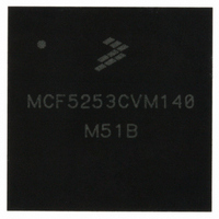
MCF5253CVM140 Freescale Semiconductor, MCF5253CVM140 Datasheet - Page 59

MCF5253CVM140
Manufacturer Part Number
MCF5253CVM140
Description
IC MPU 32BIT 140MHZ 225-MAPBGA
Manufacturer
Freescale Semiconductor
Series
MCF525xr
Datasheets
1.MCF5253VM140J.pdf
(34 pages)
2.MCF5253VM140J.pdf
(8 pages)
3.MCF5253VM140J.pdf
(648 pages)
4.MCF5253VM140J.pdf
(2 pages)
Specifications of MCF5253CVM140
Core Processor
Coldfire V2
Core Size
32-Bit
Speed
140MHz
Connectivity
CAN, EBI/EMI, I²C, QSPI, UART/USART, USB OTG
Peripherals
DMA, WDT
Program Memory Type
ROMless
Ram Size
128K x 8
Voltage - Supply (vcc/vdd)
1.08 V ~ 1.32 V
Data Converters
A/D 6x12b
Oscillator Type
External
Operating Temperature
-40°C ~ 85°C
Package / Case
225-MAPBGA
Family Name
MCF5xxx
Device Core
ColdFire V2
Device Core Size
32b
Frequency (max)
140MHz
Instruction Set Architecture
RISC
Supply Voltage 1 (typ)
1.2/3.3V
Operating Supply Voltage (max)
1.32/3.6V
Operating Supply Voltage (min)
1.08/3V
Operating Temp Range
-40C to 85C
Operating Temperature Classification
Industrial
Mounting
Surface Mount
Pin Count
225
Package Type
MA-BGA
Lead Free Status / RoHS Status
Lead free / RoHS Compliant
Number Of I /o
-
Eeprom Size
-
Program Memory Size
-
Lead Free Status / Rohs Status
Compliant
Available stocks
Company
Part Number
Manufacturer
Quantity
Price
Company:
Part Number:
MCF5253CVM140
Manufacturer:
FREESCALE
Quantity:
300
Company:
Part Number:
MCF5253CVM140
Manufacturer:
Freescale Semiconductor
Quantity:
10 000
Part Number:
MCF5253CVM140
Manufacturer:
FREESCALE
Quantity:
20 000
Company:
Part Number:
MCF5253CVM140J
Manufacturer:
Freescale Semiconductor
Quantity:
10 000
- MCF5253VM140J PDF datasheet
- MCF5253VM140J PDF datasheet #2
- MCF5253VM140J PDF datasheet #3
- MCF5253VM140J PDF datasheet #4
- Current page: 59 of 648
- Download datasheet (8Mb)
2.23.1
The TEST[2:0] inputs are used for various manufacturing and debug tests. For normal mode TEST [2:1]
should be ways be tied low. TEST0 should be set high for BDM debug mode and set low for JTAG mode.
2.23.2
The assertion of HI_Z will force all output drivers to a high-impedance state. The timing on HI_Z is
independent of the clock.
2.23.3
The internal PLL generates this PSTCLK/GPIO51 and output signal, and is the processor clock output that
is used as the timing reference for the Debug bus timing (DDATA[3:0] and PST[3:0]). The
PSTCLK/GPIO51 is at the same frequency as the core processor.
2.23.4
The debug data pins, DDATA0/CTS1/SDATA0_SDIO1/GPIO1, DDATA1/RTS1/SDATA2_BS2/GPIO2,
DDATA2/CTS0/GPIO3, and DDATA3/RTS0/GPIO4, are four bits wide. This nibble-wide bus displays
captured processor data and break-point status. Refer to
Interface,”
2.23.5
The processor status pins, PST0/GPIO50, PST1/GPIO49, PST2/INTMON/GPIO48, and
PST3/INTMON/GPIO47, indicate the MCF5253 processor status. During debug mode, the timing is
synchronous with the processor clock (PSTCLK) and the status is not related to the current bus transfer.
Table 2-13
Freescale Semiconductor
.
for additional information on this bus.
shows the encodings of these signals.
Test Mode
High Impedance
Processor Clock Output
Debug Data
Processor Status
(Hex)
JTAG operation will override the HI_Z pin.
$0
$1
$2
$3
$4
$5
$6
PST[3:0]
(Binary)
0000
0001
0010
0011
0100
0101
0110
Table 2-13. Processor Status Signal Encodings
Continue execution
Begin execution of an instruction
Reserved
Entry into user-mode
Begin execution of PULSE and WDDATA instructions
Begin execution of taken branch or Synch_PC
Reserved
MCF5253 Reference Manual, Rev. 1
NOTE
Chapter 20, “Background Debug Mode (BDM)
Definition
1
Signal Description
2-13
Related parts for MCF5253CVM140
Image
Part Number
Description
Manufacturer
Datasheet
Request
R
Part Number:
Description:
Mcf5253 Coldfire? Microprocessor Data Sheet
Manufacturer:
Freescale Semiconductor, Inc
Datasheet:
Part Number:
Description:
Manufacturer:
Freescale Semiconductor, Inc
Datasheet:
Part Number:
Description:
Manufacturer:
Freescale Semiconductor, Inc
Datasheet:
Part Number:
Description:
Manufacturer:
Freescale Semiconductor, Inc
Datasheet:
Part Number:
Description:
Manufacturer:
Freescale Semiconductor, Inc
Datasheet:
Part Number:
Description:
Manufacturer:
Freescale Semiconductor, Inc
Datasheet:
Part Number:
Description:
Manufacturer:
Freescale Semiconductor, Inc
Datasheet:
Part Number:
Description:
Manufacturer:
Freescale Semiconductor, Inc
Datasheet:
Part Number:
Description:
Manufacturer:
Freescale Semiconductor, Inc
Datasheet:
Part Number:
Description:
Manufacturer:
Freescale Semiconductor, Inc
Datasheet:
Part Number:
Description:
Manufacturer:
Freescale Semiconductor, Inc
Datasheet:
Part Number:
Description:
Manufacturer:
Freescale Semiconductor, Inc
Datasheet:
Part Number:
Description:
Manufacturer:
Freescale Semiconductor, Inc
Datasheet:
Part Number:
Description:
Manufacturer:
Freescale Semiconductor, Inc
Datasheet:
Part Number:
Description:
Manufacturer:
Freescale Semiconductor, Inc
Datasheet:


