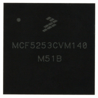
MCF5253CVM140 Freescale Semiconductor, MCF5253CVM140 Datasheet - Page 111

MCF5253CVM140
Manufacturer Part Number
MCF5253CVM140
Description
IC MPU 32BIT 140MHZ 225-MAPBGA
Manufacturer
Freescale Semiconductor
Series
MCF525xr
Datasheets
1.MCF5253VM140J.pdf
(34 pages)
2.MCF5253VM140J.pdf
(8 pages)
3.MCF5253VM140J.pdf
(648 pages)
4.MCF5253VM140J.pdf
(2 pages)
Specifications of MCF5253CVM140
Core Processor
Coldfire V2
Core Size
32-Bit
Speed
140MHz
Connectivity
CAN, EBI/EMI, I²C, QSPI, UART/USART, USB OTG
Peripherals
DMA, WDT
Program Memory Type
ROMless
Ram Size
128K x 8
Voltage - Supply (vcc/vdd)
1.08 V ~ 1.32 V
Data Converters
A/D 6x12b
Oscillator Type
External
Operating Temperature
-40°C ~ 85°C
Package / Case
225-MAPBGA
Family Name
MCF5xxx
Device Core
ColdFire V2
Device Core Size
32b
Frequency (max)
140MHz
Instruction Set Architecture
RISC
Supply Voltage 1 (typ)
1.2/3.3V
Operating Supply Voltage (max)
1.32/3.6V
Operating Supply Voltage (min)
1.08/3V
Operating Temp Range
-40C to 85C
Operating Temperature Classification
Industrial
Mounting
Surface Mount
Pin Count
225
Package Type
MA-BGA
Lead Free Status / RoHS Status
Lead free / RoHS Compliant
Number Of I /o
-
Eeprom Size
-
Program Memory Size
-
Lead Free Status / Rohs Status
Compliant
Available stocks
Company
Part Number
Manufacturer
Quantity
Price
Company:
Part Number:
MCF5253CVM140
Manufacturer:
FREESCALE
Quantity:
300
Company:
Part Number:
MCF5253CVM140
Manufacturer:
Freescale Semiconductor
Quantity:
10 000
Part Number:
MCF5253CVM140
Manufacturer:
FREESCALE
Quantity:
20 000
Company:
Part Number:
MCF5253CVM140J
Manufacturer:
Freescale Semiconductor
Quantity:
10 000
- MCF5253VM140J PDF datasheet
- MCF5253VM140J PDF datasheet #2
- MCF5253VM140J PDF datasheet #3
- MCF5253VM140J PDF datasheet #4
- Current page: 111 of 648
- Download datasheet (8Mb)
7.3.1.3
The DMR0,
Freescale Semiconductor
Address MBAR + 0x10C (DMR0)
31–18
Reset – – – – – – – – – – – – – – – – – – – – – – –
BAM
17–9
Field
Bits
WP
5–4
1–0
PM
PS
IP
8
3
2
Table 7-5. DRAM Address and Control Register (DACR0) Field Descriptions (Synchronous Mode)
W
R
31 30 29 28 27 26 25 24 23 22 21 20 19 18 17 16 15 14 13 12 11 10 9
Base address mask. Masks DACR0[BA]. Lets the DRAM controller connect to various DRAM sizes. Mask bits need
not be contiguous (see
0 The associated address bit is used in decoding the DRAM hit to a memory block.
1 The associated address bit is not used in the DRAM hit decode.
Reserved, should be cleared.
Write protect. Determines whether the associated block of DRAM is write protected.
0 Allow write accesses
1 Ignore write accesses. The DRAM controller ignores write accesses to the memory block and an address
Port size. Indicates the port size of the associated block of SDRAM, which allows for dynamic sizing of associated
SDRAM accesses.
1x 16-bit port
0x Do not use.
Initiate precharge all (
using IP should be no wider than the port size programmed in PS.
0 Take no action.
1 A PALL command is sent to the associated SDRAM block. During initialization, this command is executed after
all DRAM controller registers are programmed. After IP is set, the next write to an appropriate SDRAM address
generates the
Page mode. Indicates how the associated SDRAM block supports page-mode
operation.
0 Page mode on bursts only. The DRAM controller dynamically bursts the transfer if it falls within a single page and
the transfer size exceeds the port size of the SDRAM block. After the burst, the page closes and a precharge is
issued.
1 Continuous page mode. The page stays open and only SDCAS needs to be asserted for sequential SDRAM
accesses that hit in the same page, regardless of whether the access is a burst.
Reserved, should be cleared.
exception occurs. Write accesses to a write-protected DRAM region are compared in the chip select module for a
hit. If no hit occurs, an external bus cycle is generated. If this external bus cycle is not acknowledged, an access
exception occurs.
Figure
DRAM Controller Mask Registers (DMR0)
Table 7-6. DRAM Controller Mask Register (DMR0) Field Descriptions
7-5, includes mask bits for the base address and for address attributes.
PALL
BAM
command to the SDRAM block.
Figure 7-5. DRAM Controller Mask Register (DMR0)
PALL
Section 7.6, “SDRAM
) command. The DRAM controller clears IP after the
MCF5253 Reference Manual, Rev. 1
(continued)
Example.”)
Description
Description
WP
–
8
PALL
Synchronous DRAM Controller Module
– –
7
command is finished. Accesses
C/I AM SC SD UC UD V
6
–
5
Access: User read/write
–
4
3
–
–
2
–
1
7-7
0
0
Related parts for MCF5253CVM140
Image
Part Number
Description
Manufacturer
Datasheet
Request
R
Part Number:
Description:
Mcf5253 Coldfire? Microprocessor Data Sheet
Manufacturer:
Freescale Semiconductor, Inc
Datasheet:
Part Number:
Description:
Manufacturer:
Freescale Semiconductor, Inc
Datasheet:
Part Number:
Description:
Manufacturer:
Freescale Semiconductor, Inc
Datasheet:
Part Number:
Description:
Manufacturer:
Freescale Semiconductor, Inc
Datasheet:
Part Number:
Description:
Manufacturer:
Freescale Semiconductor, Inc
Datasheet:
Part Number:
Description:
Manufacturer:
Freescale Semiconductor, Inc
Datasheet:
Part Number:
Description:
Manufacturer:
Freescale Semiconductor, Inc
Datasheet:
Part Number:
Description:
Manufacturer:
Freescale Semiconductor, Inc
Datasheet:
Part Number:
Description:
Manufacturer:
Freescale Semiconductor, Inc
Datasheet:
Part Number:
Description:
Manufacturer:
Freescale Semiconductor, Inc
Datasheet:
Part Number:
Description:
Manufacturer:
Freescale Semiconductor, Inc
Datasheet:
Part Number:
Description:
Manufacturer:
Freescale Semiconductor, Inc
Datasheet:
Part Number:
Description:
Manufacturer:
Freescale Semiconductor, Inc
Datasheet:
Part Number:
Description:
Manufacturer:
Freescale Semiconductor, Inc
Datasheet:
Part Number:
Description:
Manufacturer:
Freescale Semiconductor, Inc
Datasheet:


