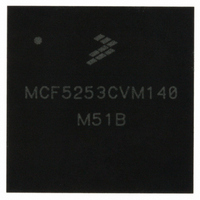
MCF5253CVM140 Freescale Semiconductor, MCF5253CVM140 Datasheet - Page 48

MCF5253CVM140
Manufacturer Part Number
MCF5253CVM140
Description
IC MPU 32BIT 140MHZ 225-MAPBGA
Manufacturer
Freescale Semiconductor
Series
MCF525xr
Datasheets
1.MCF5253VM140J.pdf
(34 pages)
2.MCF5253VM140J.pdf
(8 pages)
3.MCF5253VM140J.pdf
(648 pages)
4.MCF5253VM140J.pdf
(2 pages)
Specifications of MCF5253CVM140
Core Processor
Coldfire V2
Core Size
32-Bit
Speed
140MHz
Connectivity
CAN, EBI/EMI, I²C, QSPI, UART/USART, USB OTG
Peripherals
DMA, WDT
Program Memory Type
ROMless
Ram Size
128K x 8
Voltage - Supply (vcc/vdd)
1.08 V ~ 1.32 V
Data Converters
A/D 6x12b
Oscillator Type
External
Operating Temperature
-40°C ~ 85°C
Package / Case
225-MAPBGA
Family Name
MCF5xxx
Device Core
ColdFire V2
Device Core Size
32b
Frequency (max)
140MHz
Instruction Set Architecture
RISC
Supply Voltage 1 (typ)
1.2/3.3V
Operating Supply Voltage (max)
1.32/3.6V
Operating Supply Voltage (min)
1.08/3V
Operating Temp Range
-40C to 85C
Operating Temperature Classification
Industrial
Mounting
Surface Mount
Pin Count
225
Package Type
MA-BGA
Lead Free Status / RoHS Status
Lead free / RoHS Compliant
Number Of I /o
-
Eeprom Size
-
Program Memory Size
-
Lead Free Status / Rohs Status
Compliant
Available stocks
Company
Part Number
Manufacturer
Quantity
Price
Company:
Part Number:
MCF5253CVM140
Manufacturer:
FREESCALE
Quantity:
300
Company:
Part Number:
MCF5253CVM140
Manufacturer:
Freescale Semiconductor
Quantity:
10 000
Part Number:
MCF5253CVM140
Manufacturer:
FREESCALE
Quantity:
20 000
Company:
Part Number:
MCF5253CVM140J
Manufacturer:
Freescale Semiconductor
Quantity:
10 000
- MCF5253VM140J PDF datasheet
- MCF5253VM140J PDF datasheet #2
- MCF5253VM140J PDF datasheet #3
- MCF5253VM140J PDF datasheet #4
- Current page: 48 of 648
- Download datasheet (8Mb)
Signal Description
2-2
Chip Selects[2:0]
Buffer enable 1
Buffer enable 2
Transfer acknowledge
Wake Up
Serial Clock Line
Serial Data Line
Receive Data
Transmit Data
Request-To-Send
Clear-To-Send
Timer Output
IEC958 inputs
IEC958 outputs
Serial data in
Serial data out
Word clock
Bit clock
Signal Name
DDATA3/RTS0/GPIO4
CS0/CS4
CS1/QSPICS3/GPIO28
BUFENB1/GPIO29
BUFENB2/GPIO30
TA/GPIO12
WAKEUP/GPIO21
SCL0/SDATA1_BS1/GPIO41
SCL1/TXD1/GPIO10
SDA0/SDATA3/GPIO42
SDA1/RXD1/GPIO44
SDA1/RXD1/GPIO44
RXD0/GPIO46
EF/RXD2/GPIO6
SCL1/TXD1/GPIO10
TXD0/GPIO45
XTRIM/TXD2/GPIO0
DDATA1/RTS1/SDATA2_BS2/GPIO2
DDATA2/CTS0/GPIO3
DDATA0/CTS1/SDATA0_SDIO1/GPIO1
SDATAO1/TOUT0/GPIO18
EBUIN1/GPIO36
EBUIN2/SCLKOUT/GPIO13
EBUIN3/CMD_SDIO2/GPIO14
QSPICS0/EBUIN4/GPIO15
EBUOUT1/GPIO37
QSPICS1/EBUOUT2/GPIO16
SDATAI1/GPIO17
SDATAI3/GPIO8
SDATAO1/TOUT0/GPIO18
SDATAO2/GPIO34
LRCK1/GPIO19
LRCK2/GPIO23
LRCK3/AUDIOCLK/GPIO43
SCLK1/GPIO20
SCLK2/GPIO22
SCLK3/GPIO35
Table 2-1. MCF5253 Signal Index (continued)
Mnemonic
MCF5253 Reference Manual, Rev. 1
Chip selects bits 2 through 0—
enable peripherals at programmed
addresses. CS0 provides boot ROM
selection.
Two programmable buffer
enables—allow seamless steering of
external buffers to split data and
address bus in sections.
Transfer Acknowledge signal.
Wake-up signal input
Clock signal for Dual I
operation
Serial data port for second I
operation
Receive serial data input for UART
Transmit serial data output for UART
Signals sent from UART0/1 that it is
ready to receive data
Signals sent to UART0/1 that data can
be transmitted to peripheral
Capability of output waveform or pulse
generation
Audio interfaces to IEC958 inputs
Audio interfaces to IEC958 outputs
Audio interfaces to serial data inputs
Audio interfaces to serial data outputs
Audio interfaces to serial word clocks
audio interfaces to serial bit clocks
Function
2
C module
2
C module
Freescale Semiconductor
Output
Input/
In/Out
In/Out
In/Out
In/Out
In/Out
In/Out
In/Out
In/Out
In/Out
Out
Out
Out
Out
Out
Out
In
In
In
In
In
negated
Reset
State
–
–
–
–
–
–
–
–
–
–
–
–
–
–
–
–
–
Related parts for MCF5253CVM140
Image
Part Number
Description
Manufacturer
Datasheet
Request
R
Part Number:
Description:
Mcf5253 Coldfire? Microprocessor Data Sheet
Manufacturer:
Freescale Semiconductor, Inc
Datasheet:
Part Number:
Description:
Manufacturer:
Freescale Semiconductor, Inc
Datasheet:
Part Number:
Description:
Manufacturer:
Freescale Semiconductor, Inc
Datasheet:
Part Number:
Description:
Manufacturer:
Freescale Semiconductor, Inc
Datasheet:
Part Number:
Description:
Manufacturer:
Freescale Semiconductor, Inc
Datasheet:
Part Number:
Description:
Manufacturer:
Freescale Semiconductor, Inc
Datasheet:
Part Number:
Description:
Manufacturer:
Freescale Semiconductor, Inc
Datasheet:
Part Number:
Description:
Manufacturer:
Freescale Semiconductor, Inc
Datasheet:
Part Number:
Description:
Manufacturer:
Freescale Semiconductor, Inc
Datasheet:
Part Number:
Description:
Manufacturer:
Freescale Semiconductor, Inc
Datasheet:
Part Number:
Description:
Manufacturer:
Freescale Semiconductor, Inc
Datasheet:
Part Number:
Description:
Manufacturer:
Freescale Semiconductor, Inc
Datasheet:
Part Number:
Description:
Manufacturer:
Freescale Semiconductor, Inc
Datasheet:
Part Number:
Description:
Manufacturer:
Freescale Semiconductor, Inc
Datasheet:
Part Number:
Description:
Manufacturer:
Freescale Semiconductor, Inc
Datasheet:


